Registration of public notification
If you register your e-mail address, we will notify you when the latest issue is published. If you wish, please register from the registration form. To delete your registration, please visit here.
October 2024 No.99
With the advancement of autonomous driving and vehicle electrification, the number of onboard sensors is expected to increase. Powering each sensor via wired connections can lead to increased costs and weight due to power and communication cables. This paper investigates wireless power transmission using a spatial transmission method to supply power to each sensor. We confirmed that a temperature sensor embedded in the headrest could operate at 30-second intervals using wireless power transmission at a transmission frequency of 920 MHz and a transmission power of 1W. In addition, we simulated the distribution of electric field intensity inside the vehicle cabin and confirmed that the electric field intensity required for the sensor to operate could be achieved in most areas of the cabin.
3.4 MB

3.4 MB
For the realization of autonomous driving, 5G is expected to be used due to its superior features such as high speed, large capacity, and low latency capabilities. To enable large-scale data communication, such as sensing information transmission, it is desirable to use the millimeter-wave band, which has a bandwidth of several hundred megahertz in 5G. 5G millimeter-wave antennas use beamforming technology to transmit radio waves over long distances. We set up a scenario where a vehicle equipped with a 5G millimeter-wave antenna communications with a base station and performs beamforming control while driving, and dynamically evaluated it using 5G signals. This paper reports the evaluation method and results based on the proposed scenario.
3.9 MB

3.9 MB
The long-term reliability of optical fibers heavily depends on the durability of the protective coating layers surrounding the glass fiber. The physical properties of the inner layer coating, such as Young's modulus and gel fraction are crucial to the durability. Ultraviolet light (UV) curable resins are commonly used for coating, and accurate prediction of the physical properties under different irradiation condition is essential for optimizing the manufacturing process. However, the complex reaction mechanism involved in UV irradiation-induced radical polymerization poses challenges in accurately modeling these properties. In this study, we presents an analytical formula based on chemical reaction kinetics to determine the concentration of photoinitiators. Moreover, we successfully predict coating properties by utilizing a calibration curve that compares the photoinitiator consumption rate with the coating properties after the curing process.
1.7 MB

1.7 MB
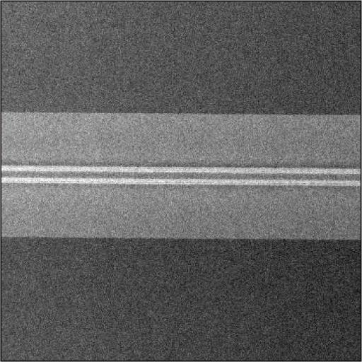
To meet the rapidly increasing demand for optical communication traffic, a high-capacity solution is required through the high-density integration of optical devices. The challenge lies in the potential degradation of device performance due to heat generation. Consequently, there is a need for a semiconductor laser exhibiting superior temperature attributes. Addressing this, we have developed a 1.3 µm-wavelength laser, employing a GaInAs/GaAsSb/GaInAs type-II active layer on a GaAs substrate, suitable for optical communication. This has been achieved utilizing our proprietary low-temperature growth technology from highly productive Organic-Metal Vapor Phase Epitaxy. Our solution exhibits a characteristic temperature of the threshold current density of 152 K between 25°C and 100°C, a value significantly larger than the traditional 60 K of InGaAsP lasers on InP substrates. This result demonstrates the feasibility of a 1.3 µm semiconductor laser with a type-II active layer, less susceptible to performance degradation in high-temperature environments.
1.4 MB
1.4 MB
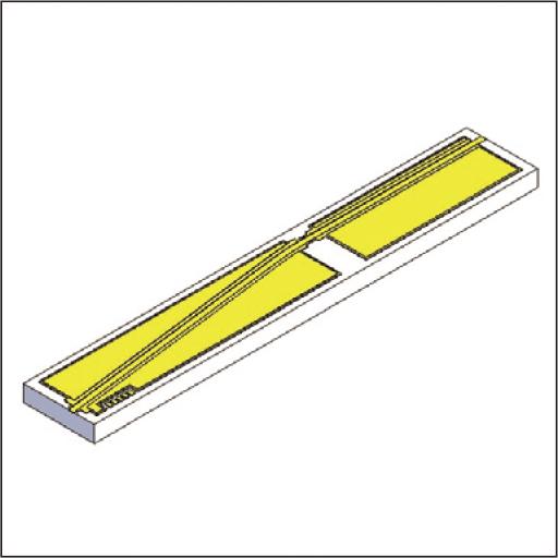
The growing demand for generative AI and high-performance computing has increased the importance of high-speed, energy-efficient communications in data centers, leading to an increased focus on co-packaged optics (CPO). The external laser sources (ELSs), a component of CPO, require high optical output power of several hundred mW and low power consumption with power conversion efficiency greater than 20%. This paper discusses the integration of a wide stripe waveguide semiconductor optical amplifier (SOA) into a 1.3 μm high-power semiconductor laser for CPO. By using an electrically isolated structure for each element, we have optimized the power distribution to achieve over 400 mW output power and 25% power conversion efficiency at a temperature of 45℃.
1.6 MB
1.6 MB
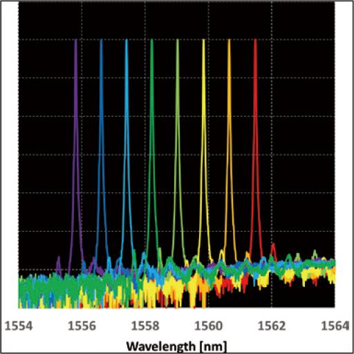
This paper presents our development of an 8-wavelength tunable electro-absorption modulator integrated laser, designed for mobile and access networks. The laser was created in response to the increased data traffic and data rate demands within 5G mobile fronthaul communication networks, particularly in areas with limited fiber infrastructure. This solution addresses the growing need for wavelength tunable optical transceivers and supports the adoption of wavelength division multiplexing. The performance of the laser was evaluated in a compact 25 Gbit/s dense wavelength division multiplexing (DWDM) transceiver, housed in an SFP28 form-factor.
1.8 MB
1.8 MB
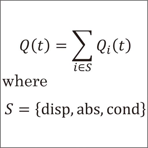
This paper focuses on the “Current Integration Method (Q-t method),” widely used in Japan in recent years, to understand the electrical conduction and space charge behavior of insulating materials, in conjunction with the advancement of high voltage direct current (HVDC) technology and polymer insulation technology. The Q-t method involves connecting an integrating capacitor to the sample in series and measuring the integrated small currents passing through it. The advantage of this method is that it allows comprehensive and panoramic observation of electrical phenomena, and by applying this advantage to dielectric measurements, it enables a wide range of applications such as condition monitoring, understanding the limits of insulation material usage, material selection and evaluation. This paper provides examples of its applications and highlights its unique advantages and functionality.
1.7 MB
1.7 MB
The Nissin Electric Group has been enhancing manufacturing capabilities and improving productivity as part of its medium-to-long-term business plan VISION2025. Our main goal is to improve productivity by strengthening our manufacturing technology. Under the slogan “NISSIN ISSIN” (i.e., Nissin renewal), we have been promoting the smartification of our factories through activities that spin the dual wheels of expanding and inheriting important artisan skills and techniques, while also advancing projects that focus on NPS efficiency and the use of cutting-edge technologies. This paper presents an overview of these efforts.
4.4 MB

4.4 MB
Nissin Electric Co., Ltd.'s equipment and parts solution business utilizes Nissin Electric Group's power equipment manufacturing technology for the contract manufacturing of equipment parts for various industries. Established in 2000 at Nissin Electric (Thailand) Co., Ltd. (NET), this business has expanded its manufacturing bases to Vietnam and Myanmar, supplying equipment and parts worldwide. Since its foundation, Nissin Electric has consistently improved its manufacturing capabilities. This paper describes the manufacturing technology used in the equipment and parts solution business.
2 MB

2 MB
Automotive components have complex designs and thin walls, for weight reduction. In recent years, such materials are becoming increasingly difficult to cut due to their high strength. Meanwhile, there has been a growing demand for high-speed and high-efficiency machining to reduce lead time. Under these circumstances, customers need cutting tools that have long tool life and stable cutting performance. To satisfy these demands, we have developed the new coated grade AC4125K for cast iron turning. This paper describes the features and cutting performance of AC4125K.
4.7 MB
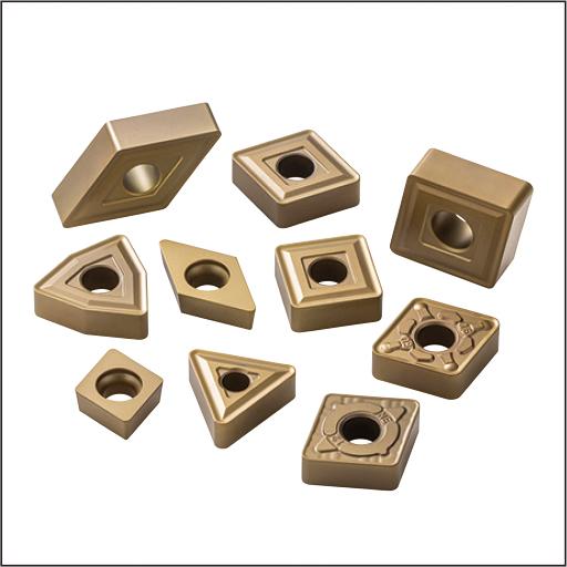
4.7 MB
Scanning transmission electron microscopy (STEM), characterized by its high spatial resolution, is a indispensable tool for atomic-level structural analysis of crystalline materials. Particularly in polycrystalline materials such as metals and ceramics, grain boundaries often determine material properties. However, due to the randomness of grain orientations, efficient extraction of grain pairs for grain boundary analysis has been a challenge. In response, we have developed a new technique for crystal orientation analysis using electron backscatter diffraction (EBSD). By applying two types of EBSD methods, reflective and transmission, to sintered tungsten carbide (WC) and cobalt (Co), we confirmed that transmission EBSD can find suitable grain pairs with practical throughput. In addition, STEM analysis successfully detected step structures and Co segregation at WC grain boundaries. The integration of STEM and EBSD analysis developed in this study presents a highly effective approach to structural analysis of polycrystalline grain boundaries for material property improvement.
4.8 MB
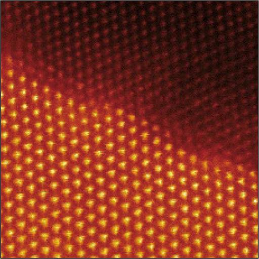
4.8 MB
In recent years, technological developments have increased the demand for high-performance radar. Electron tubes and low-power, low-frequency semiconductor elements have been used in the past, but gallium nitride high-electron-mobility transistors (GaN HEMTs), which are optimized for high power and high frequency, are being adopted to increase radar detection range and improve accuracy.
1.1 MB
Cemented carbide, a hard alloy primarily composed of tungsten carbide powder (hereinafter referred to as “WC powder”), is widely used in various fields such as the automotive, aerospace, and electronics industries, due to its high hardness and wear resistance, which can reduce processing costs and time when used as cutting tools. With the increasing demand for multi-functional and high-performance components in recent times, there is a growing need for high-precision tools, prompting the demand for cemented carbides made from fine-particle WC powder that can achieve sharp shapes.
1.2 MB
Copyright of the paper contained in SUMITOMO ELECTRIC TECHNICAL REVIEW belongs to Sumitomo Electric Industries, Ltd.
The paper is to be used solely for private, reference purpose, and reproduction without the permission of the copyright holder is prohibited.
Meet the Authors of the SUMITOMO ELECTRIC TECHNICAL REVIEW
We at Sumitomo Electric Group are driven to pursue technological innovations to create value for a better world.
Learn more
