Development History of the Ion Implanter IMPHEAT
Going ahead of the times, taking on new challenges, and creating new products
Challenges Associated with Different Ion Implantation Processes on Si and SiC
In 2009, Sumitomo Electric approached NIC about developing an ion implanter for SiC power devices. Sumitomo Electric, grasping the demands of the times for EVs, focused on the potential of SiC and had high hopes that NIC’s ion implantation technology would serve as the catalyst for the creation of new power devices. Although the NIC technical team had knowledge of the excellent basic properties of SiC, many of them shared the view that ion implantation was technically difficult.
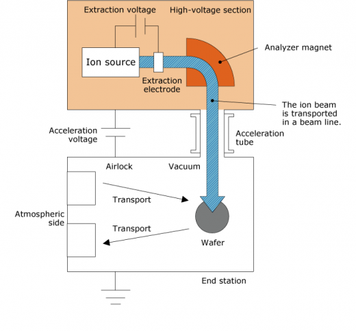
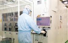
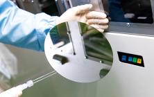
An ion implanter consists of an ion source, which generates ions of the element to be implanted; an analyzer magnet, which separates multiple types of ions based on differences in mass and charge; an acceleration tube, which accelerates the ions to a specified energy; and an end station, which implants the ions into the wafer. However, there are significant differences between ion implantation on Si and SiC. First of all, the wafers themselves are different. While Si wafers have a high degree of flatness, SiC wafers have a low degree of flatness and are easily deformed by the effects of ion implantation and heat. Additionally, the wafer temperature during implantation is below 100°C with Si, but SiC requires heating to around 500°C. Furthermore, while the ion species implanted in Si were boron, phosphorus, and arsenic, in SiC it was necessary to implant aluminum in addition to phosphorus.

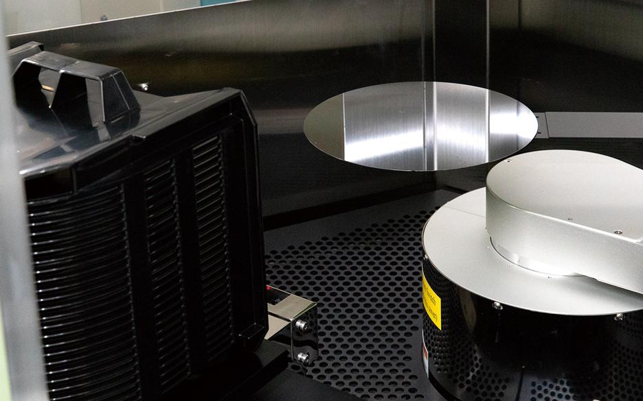
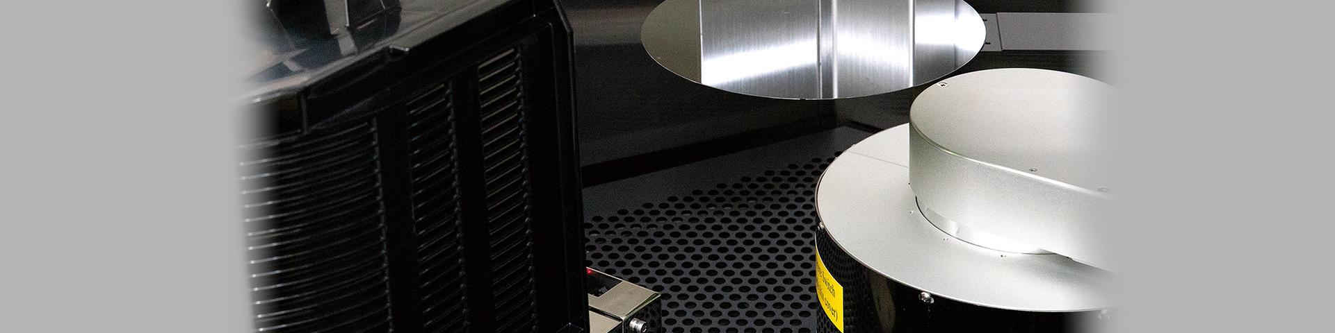
Transport System Takes on High- Temperature Ion Implantation
At the time, the people who took on these challenges were the technical team currently responsible for providing technical support for installed products handled by NIC. While there were many challenges to overcome in developing an ion implanter for SiC power devices, the most pressing problem was related to high-temperature ion implantation, a notable difference from ion implanters for Si power devices. Shiro Shiojiri, a member of the technical team and responsible for developing a wafer transport system, encountered the major obstacle of high temperatures.
“Compared to Si, SiC has a unique problem in that it is difficult to repair defects in the crystal after ion implantation, so the challenge was to suppress the generation of defects during implantation. To achieve this, it was necessary to heat the SiC wafer to around 500°C while implanting ions. However, since the transport system had many components that are sensitive to heat, one of the challenges was how to insulate them from heat. I struggled to find a mechanism that would physically block heat and prevent it from spreading to the surrounding area,” says Shiojiri.
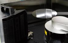
The SiC wafer transport system remains one of the development challenges. In addition to being able to withstand high temperatures, achieving stable transport was also a major challenge. Tomoaki Kobayashi, who currently works as an expert, was also involved in the transport system and high-temperature protection measures.
“In early SiC implanters, wafers were placed on the holder by hand. For transportation, an electrostatic chuck was used, which uses electrical force to attract and hold the holder. It was necessary to consider the insulation between the power to the electrostatic chuck and the power to the high-temperature heater, as well as the appropriate voltages. There were also many challenges to overcome, such as how to raise the temperature quickly, how to achieve an even temperature distribution, and how to measure the temperature. We continued to make steady efforts to overcome these challenges one by one,” says Kobayashi.
Kazuki Tobikawa was in charge of developing the high-temperature electrostatic chuck that Kobayashi mentioned and of measuring the wafer temperature.
“An electrostatic chuck is a component that attracts the wafer. We found that its attraction was rapidly lost at high temperatures. Thermal expansion caused the electrostatic chuck to warp, creating a gap between the wafer and the electrostatic chuck, reducing the attraction and making stable transportation difficult. So we aimed for stable transportation through trial and error, for example by attaching a sliding mechanism to the electrostatic chuck to suppress warping. Regarding temperature measurement, we sought cooperation from a radiation thermometer manufacturer building radiation thermometers for non-contact measurements, and we could solve the problem,” explains Tobikawa.
Aluminum Ions Required for SiC Power Devices
Ion implanters for SiC power devices need to ionize aluminum, which is not normally used. Ionization converts gas or vapor containing the intended material into plasma, but there is no such gas that contains elemental aluminum. The person who took on this challenge was Tetsuya Igo, who is currently in charge of technical sales in the Semiconductor Equipment Division.
“We repeatedly considered what type of aluminum compound would be good to use. And we turned our attention to aluminum nitride. By applying a plasma of a gas containing fluorine to aluminum nitride, aluminum fluoride was generated, and an aluminum ion beam was successfully generated. The key was how to stabilize it. The high voltage applied caused discharges and made the beam generation unstable. Another challenge was to develop an aluminum ion source that could produce large amounts of aluminum ions for a long period of time. This was passed down as a task for the future,” says Igo.
Thus, the first research unit was delivered. However, problems arose to the point that the team members had to commute to the client, Sumitomo Electric, for a year. The issues and new challenges discovered there led to the development of the mass-produced machines IMPHEAT and IMPHEAT-II as well as the next-generation ion implanter.
NEXT
Creation and Evolution: The Inherited Spirit of the Development Staff
- Reaching out to the next generation with a desire to contribute to society -
Registration of public notification
If you register your e-mail address, we will notify you when the latest issue is published. If you wish, please register from the registration form.
To delete your registration, please visit here.