SiC Power Devices Inspire High Expectations for Efficient Electricity
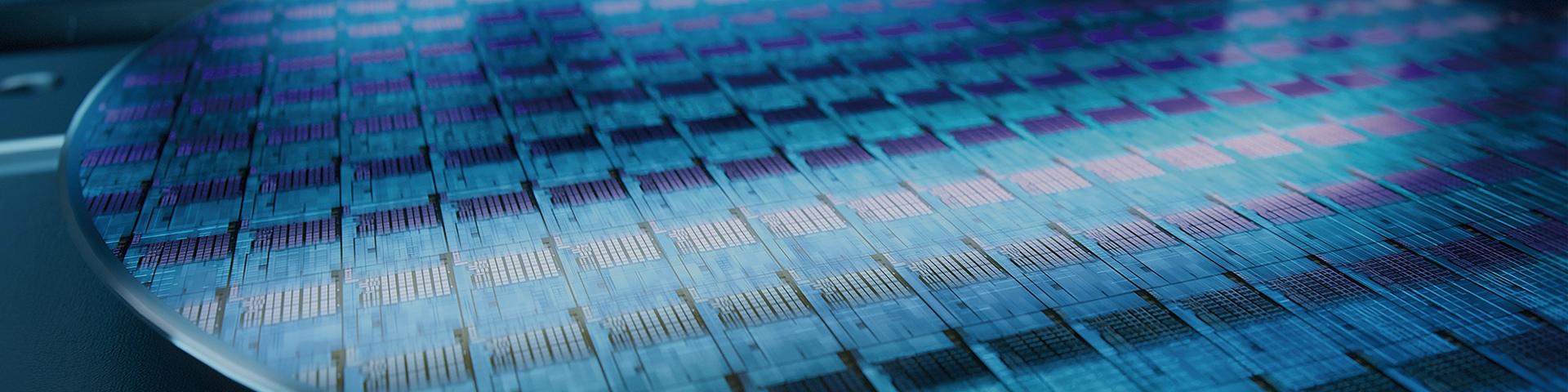
A semiconductor wafer and manufactured transistors (rendered image)
Ion implantation technology is essential for manufacturing
The Challenge of Power Loss During Power Conversion
We use electricity every day. That electricity is generated by fossil fuels, hydro, nuclear, solar, or wind power, but the generated electricity cannot be used as is. Processes carried out between power generation and consumption include power conversion changing AC to DC and DC to AC, frequency conversion of AC, voltage and current regulation, and switching to turn the power on and off. Such high-voltage and high-current processes are controlled by power devices. Power devices are used in a wide range of sectors, from social infrastructure to everyday home appliances. The problem is that this control process always involves power loss. By reducing this loss as much as possible, it becomes possible to significantly reduce total greenhouse gas emissions.
While silicon (Si) has traditionally been widely used for power device wafers, in recent years, SiC has been attracting attention. Its excellent basic properties are clear when compared with Si. It has one-tenth the resistance, three times the thermal conductivity and high-frequency characteristics, and 10 times the high breakdown voltage of Si, and can operate at high temperatures of over 200°C. This allows the power module to be made smaller and lighter with lower power loss.
Injecting Ionized Impurities into Wafers
Take EVs as an example. Many power devices are used in high-voltage DC batteries, the AC motor that drives the vehicle, and charging stations to convert between DC and AC power and between high and low voltages. Use of SiC significantly improves the environmental efficiency of the car, by not only reducing loss but also enabling the car to be smaller and lighter and simplifying the cooling system.
Manufacturing power devices requires several hundred process steps. One of the manufacturing process steps is ion implantation, which is performed by an ion implanter. What is ion implantation?
An ion is an atom that carries an electric charge. Atoms are originally neutral, but by transferring negatively charged electrons, atoms become ions with a negative or positive charge. The ion implanter converts a gas or vapor containing boron, phosphorus, arsenic, aluminum, or the like into plasma. After being ionized and high-voltage accelerated, ions are implanted into a wafer. In other words, ion implantation involves bombarding the wafer with ionized impurities. Introducing the appropriate amount of impurities controls the electrical characteristics of power devices. Ion implantation is used in the manufacturing process of power devices to improve wafer conductivity and electron mobility, form p-type and n-type semiconductors* and fine integrated circuits, optimize device performance, and build devices with different characteristics. It has become an indispensable technology that plays an important role in the power device manufacturing process.
* p-type and n-type semiconductors: A p-type (positive) semiconductor is one in which electrical conduction occurs due to electrons moving to holes, while an n-type (negative) semiconductor is one in which electrical conduction occurs due to free electrons with a negative charge. Combinations of these semiconductors are the basic constituents of electronic devices.
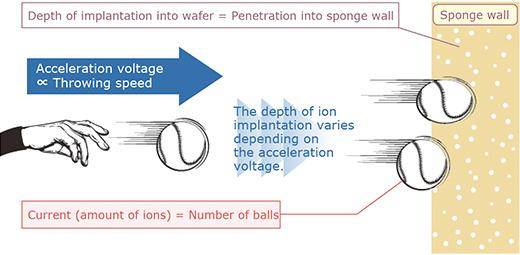
Fig. 1: Ion implantation involves the implantation of impurities called donors, which provide electrons, and acceptors, which receive electrons, into a wafer, which is an insulator in which electrons do not move freely. The process is like throwing balls (ionized impurities) into a sponge wall (wafer). By changing the speed and number of ions, it is possible to control the electrical characteristics of the power device, creating a usable semiconductor tailored to the purpose.
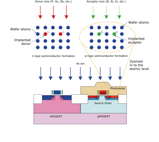
Fig. 2: Ion implantation is one of the process steps in semiconductor manufacturing, including photoresist application, exposure and development, etching, resist stripping and cleaning, and planarization. By repeating these process steps while changing the circuit pattern, donor, and acceptor, electronic devices with a structure like the one shown in the cross-sectional view are formed on the wafer.
Ion Implantation Technology Developed over Many Years
Nissin Ion Equipment Co., Ltd. (NIC) develops and manufactures ion implanters. The company was spun off in 1999 from Nissin Electric Co., Ltd., another member of the Sumitomo Electric Group. NIC is headquartered in Kyoto, Japan and has a development and production site in Shiga. In addition, the company conducts business globally with its sites based in Singapore, China, South Korea, the United States, and other countries. The company began producing ion implanters in the 1970s, when it was still part of Nissin Electric, and its epoch-making business began in the late 1980s with the launch of its ion implanters for flat panel displays (FPDs) and in the early 2000s with the start of production of the EXCEED family of mass-produced silicon ion implanters. Subsequently in 2009, the company became the first in the world to undertake the development of ion implanters for SiC power devices. A person who has led the evolution of these ion implanters is President Nobuo Nagai.
EXCEED and IMPHEAT are trademarks or registered trademarks of Nissin Ion Equipment Co., Ltd.
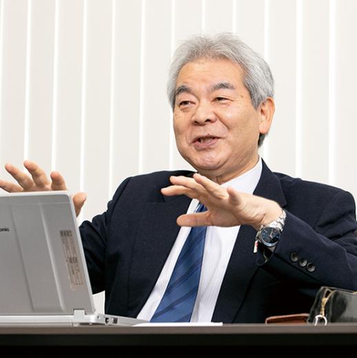
“In line with the progress in the SDGs, environmental impact reduction, and other global trends, SiC has long been a focus of attention as a power device wafer material. However, its application has been difficult for many years due to technical difficulties, high costs, and other issues. Nevertheless, as the demand of the times has turned to ecosystems, the conditions are now in place to make SiC power devices a reality. Leveraging the technology we have developed over many years in the development and manufacturing of ion implanters for very large scale integration (VLSI), we first developed a high-temperature ion implanter tailored for SiC power devices in 2009 for research use. Subsequently, in 2013, we released IMPHEAT, the industry’s only mass production system at the time and offered it to power device manufacturers. Furthermore, in 2019, we launched an upgraded version of the machine, IMPHEAT-II, which has been highly praised by many." (Nagai)
However, IMPHEAT-II was not meant to be the ultimate ion implanter for SiC power devices. Nagai says, “There is no end to our efforts in pursuit of higher performance.” Indeed, many challenges remain to be overcome in order to precisely meet market needs. In the following chapters, you will look at the development of the first unit, all the way up to the current efforts.
NEXT
Development History of the Ion Implanter IMPHEAT
- Going ahead of the times, taking on new challenges, and creating new products -
Registration of public notification
If you register your e-mail address, we will notify you when the latest issue is published. If you wish, please register from the registration form.
To delete your registration, please visit here.