Fθ Lens and DOE Delivered through Marketing-First Approaches
Evolution of optical design technology boosting laser processing technology
High-performance Fθ lens required for high-speed micromachining
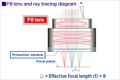
In today’s electronics-based world, demand is high for smaller, lighter and higher-performance electronic devices including smartphones. The process of manufacturing the electronic components incorporated in these devices uses laser processing machines. It is essential for these machines to be capable of highprecision, ultrafine drilling. For example, printed circuit boards in the latest smartphones, whichever the processed portion is, require drilling performed with a hole diameter of 50μm or less, which is thinner than a human hair, and a hole position deviation of 5μm or less from the target position. The Fθ lens was developed to enable highprecision drilling at these levels. Even if the laser beams strike the surface at an angle, the lens focuses the beams to a tiny spot almost perpendicular to the flat processing area to achieve uniform holes.

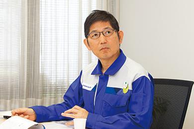
To provide high performance at this level, the Fθ lens is a lens system combining several lenses. Moreover, to control aberration, the Fθ lens generally incorporates aspherical lenses. Takashi Araki of Laser Optics Department of Sumitomo Electric Hardmetal Corporation was involved in the development of the groundbreaking Fθ lens.

“The state-of-the-art laser drilling system processes at a rate of 4,000holes per second. To enable such highspeed processing, the Fθ lens is required to offer a wide processing area and light convergence to the smallestpossible diameter (focal point size). However, to provide a wide processing area, the converging beam diameter (focal point size) generally increases, making focal distortion greater in the processing area. In short, there was a trade-off between these two requirements. As a solution to this challenge, it was necessary to use high-precision aspherical lenses and minimize errors in combining several lenses.
High-performance lenses are susceptible to manufacturing errors, tending to result in variations in performance. I worked out a robust optical design with sufficient manufacturing tolerances for individual lenses so as not to result in poor light convergence properties, even with manufacturing errors.
Highly integrated circuit (IC) package boards require the highestprecision drilling. In high-density wiring, the drilled holes, if distorted, present the risk of electric conduction failure. The history of the Fθ lens is an achievement of increasingly higher precision drilling made possible by feeding back customers’ drilling results to the design and making successive improvements. I am proud that the Fθ lens was developed and has grown as a result of a concerted effort between our customers and us. I believe that the Sumitomo Electric Group holds the world’s top technical prowess and market share for Fθ lenses for processing high-performance printed circuit boards incorporated in smartphones and highly integrated circuit package boards. Presently, I am working to increase customer satisfaction by inspecting manufactured Fθ lenses under conditions as close as possible to actual operating conditions,” says Araki.
DOE controls laser beams in the required manner
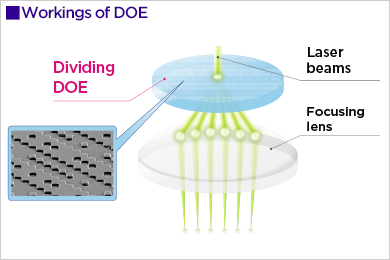
A lens or mirror directs the incident beams to converge or reflects them in another direction. Some optical components for laser have other special functions. A typical example is the diffractive optical element (DOE), which uses diffraction of light to control beams in a way not possible with any conventional lens or mirror. For example, a DOE can change the focal shape and intensity in various ways. Moreover, it can divide a beam into many beams. Hirohito Nishi, who has been studying the diffraction of light waves since he was a college student, works on designing DOEs.

“Conventional optical designs have been based on the concept of geometrical optics, which describes light propagation in terms of rays. In contrast, DOE designs are based on physical optics, which treats light as waves. A DOE has a mosaic-like raised or sunken microstructure on the surface designed through simulation to render a diffraction phenomenon. Wave optics involves highly demanding computational operations. Use of Sumitomo Electric’s proprietary design software developed in step with the evolution of the speed and capacity of computers has enabled us to respond to customer design needs in a timely fashion,” says Nishi.

The DOE divides one beam into multiple beams and enables simultaneous processing at multiple spots. It contributes to remarkable improvements in mass production capacity for the manufacturing of leadingedge electronic components. It is also effective in improving the quality of laser welding, so its practical uses are progressing in the area of automotive parts.
These high-performance optical components are made possible by constituent technologies that include materials, processing and coating technologies.

NEXT
Three key processes: synthesis, processing and coating
Pursuing high quality, high precision and high performance
Registration of public notification
If you register your e-mail address, we will notify you when the latest issue is published. If you wish, please register from the registration form.
To delete your registration, please visit here.
