Develop lenses that can withstand ultra-high-power laser beams!
Participating in a national project designed to boost the use of lasers
Development of a ZnSe focusing lens for CO2 laser processing
From 1979 through 1984, a national project drawn up by the Ministry of International Trade and Industry (current Ministry of Economy, Trade and Industry) conducted research and development of manufacturing systems incorporating ultra-high performance lasers. The project invited various businesses from different areas of specialization including laser oscillators, mechatronics and system construction. The Sumitomo Electric Group also took part in the project. The Group’s mission was to develop optical materials.
At the time, the only laser capable of delivering a high level of power suitable for laser processing was the CO2 laser.*1 To use laser beams, a focusing lens was required to concentrate the beams to an extremely small spot for high energy density. This implied the need to develop a transparent material that would withstand high-power beams. The wavelength of a CO2 laser is 10.6 μm. One candidate material with high transmittance at this wavelength was the artificial zinc selenide (ZnSe) crystal.*2
*1: A laser oscillator that uses carbon dioxide gas (CO2) as a medium. The CO2 laser was put into practical use early to process a wide range of materials such as metal, plastics, fabric, glass, lumber, concrete and paper (by, for example, cutting, welding, drilling, marking and surface modification). The majority of laser processing machines are CO2 lasers.
*2: Currently, various lasers are available that emit beams of different wavelengths. Accordingly, lenses need to be made of a wavelength-specific hightransmittance material. Typically, ZnSe is used with 10.6μm wavelength CO2 lasers, and synthetic fused silica is used with 1.07 μm wavelength fiber lasers.


ZnSe synthesis technology established
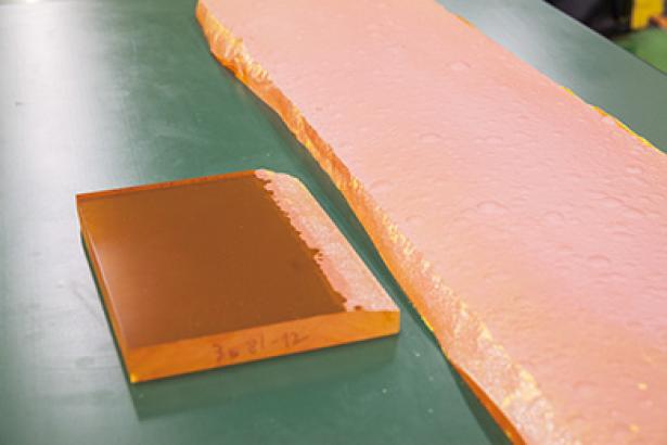
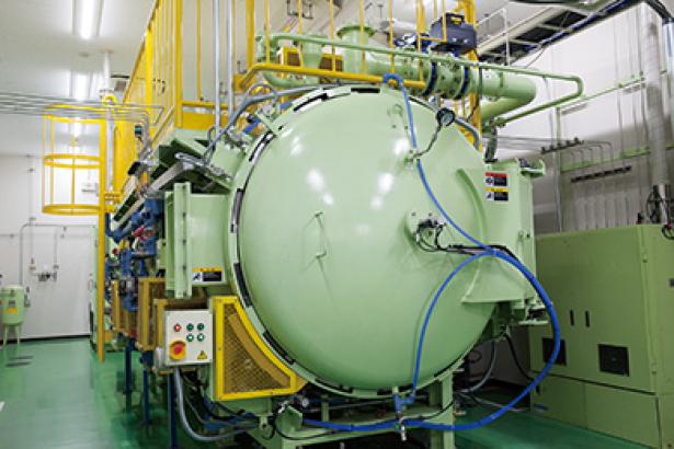
In 1980, Hirokuni Namba of the R&D Unit of Sumitomo Electric Industries, Ltd. began to take charge of the development of ZnSe synthesis technology. Drawing on his previous experience in materials research with a focus on superconductors and optical crystal materials, he addressed the challenges of ZnSe synthesis using chemical vapor deposition (CVD) to combine hydrogen selenide gas and zinc vapor. The CVD method was thought of as a thin-film forming technology, feeding a raw material gas onto a substrate placed in a reactor and gradually depositing films through chemical reaction. Forming an ingot (plate crystal) of a sufficient size and thickness for making a lens by continuing the deposition incessantly for several weeks was very challenging.

“Luckily enough, the company had a wealth of technologies built up previously through research on gallium arsenide, a compound semiconductor. I borrowed a small CVD experimental system that was not being used and conducted preliminary experiments. The experiments provided useful findings for designing a reactor to conduct full-scale research. First of all, to ensure stable crystal production, it was important to design a gas introduction path that could control turbulent gas flows. However, the CVD process involved several different control parameters, such as temperature, flux and gas pressure. Moreover, the project period did not allow the time or support the cost of experimenting with the individual parameters.
I observed, analyzed and evaluated synthesized crystals in great detail. Making full use of the knowledge and wisdom on material properties provided by interested people, I racked my brains to work out conditions for the next experiments. Those were extremely hard days. Then, finally in 1984, I had success in producing an ingot (plate crystal) of ZnSe with a sufficient size and thickness that could withstand a highpower laser beam,” recalls Namba.
In 1985, Sumitomo Electric installed a line of production equipment for synthesis, polishing and coating, and launched the ZnSe lens. In 1990s, it promoted the business on a full scale. However, the results were not satisfactory. At the time, although CO2 lasers came into wide use for cutting sheet metal, the demand was still small. The ZnSe lens business itself failed to achieve substantial results. Notwithstanding this situation, the staff visited customers frequently, listened to the purposes and uses they required for their CO2 lasers, and made their best efforts as an optical component manufacturer to respond to those needs. These efforts by the staff laid the foundation for the subsequent optical component business of the Sumitomo Electric Group. It is a shared philosophy for us to propose solutions with customized high value-added products. Various products were developed successively, including parabolic mirrors and watercooled mirrors for high-power lasers to meet the needs of steelmakers, scanners for welding body sheet steel for automakers, and coated products with controlled transmittance and light polarization properties for oscillator manufacturers.
The staff continued searching for ways to expand the business. To achieve satisfactory results, they had to wait until 1996 when they had success developing the ZnSe Fθ (F theta) lens for CO2 lasers.
“The Fθ lens for CO2 lasers was far ahead of our competitors. It was the result of our enterprising spirit and original technology. We were proud of the range of our technologies, which were seen as the world’s best at the time, that we used to develop, design and process optical components to meet emerging needs. I believe Sumitomo Electric’s technologies still remain the world’s best. In the future, I expect those technologies to produce various optical components for lasers, including fiber lasers,” says Namba.

NEXT
Evolution of optical design technology boosting laser processing technology
Fθ Lens and DOE Delivered through Marketing-First Approaches
Registration of public notification
If you register your e-mail address, we will notify you when the latest issue is published. If you wish, please register from the registration form.
To delete your registration, please visit here.
