
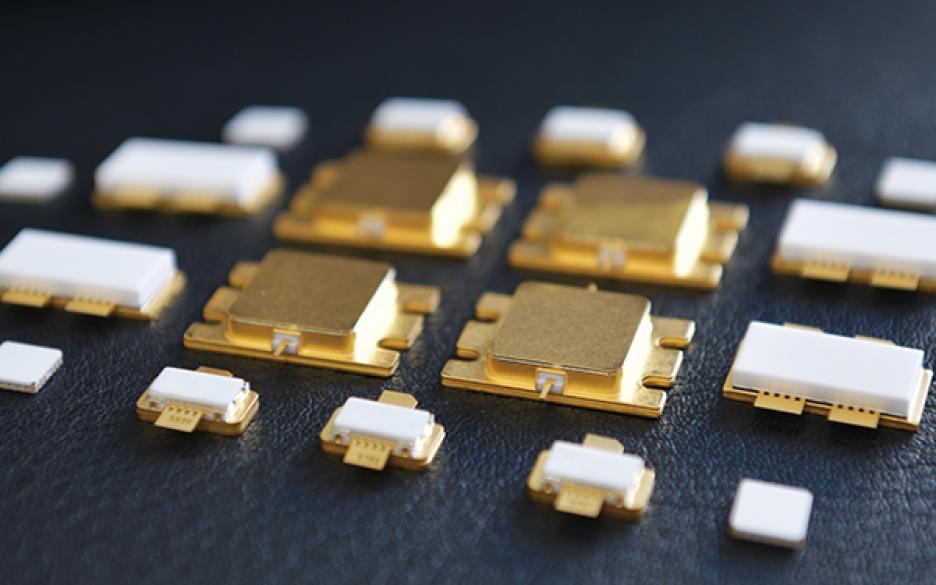
GaN HEMTs, electronic devices indispensable in the era of 5G
In Japan, the commercial service of 5G mobile communication, which is mainly used for mobile phones, started in some areas in the spring of 2020. Characterized by high speed, large capacity, low latency, and simultaneous connectivity, 5G mobile communication is expected to significantly change our daily lives and society. 5G communication requires transistors (i.e., electronic devices) that enable processing of electric signals at high speed with high output and low power consumption. The Sumitomo Electric Group was quick to start a study on new electronic devices with the future of telecommunications in mind. It focused on a material called gallium nitride (GaN), whose material properties are superior to those of conventional silicon, and developed GaN HEMTs characterized by both high speed and high output by combining GaN with High Electron Mobility Transistors (HEMTs). In 2007, the Sumitomo Electric Group marketed GaN HEMTs, which were used for 3G base stations. The GaN HEMTs were highly evaluated in the market and have evolved into products for 4G and 5G. The ATRC has contributed significantly to this evolution.
Process damage that occurs in the manufacturing operations
Yoshihiro Saito, a senior assistant manager of the Yokohama Analysis Dept. of the ATRC, has been engaged in the development of devices for 16 years since joining the company. He has been working on various analysis activities by taking full advantage of his experience. Uneven quality is one of the issues in manufacturing devices. As devices go through many steps, their characteristics change slightly. The manufacturing process of GaN HEMTs can be simply explained as follows: Epitaxy (a phenomenon in which single crystals grow in the same crystal orientation) technique is used to grow single crystals of GaN and aluminum gallium nitride (AlGaN) on substrates, and electrodes are attached in the final step.
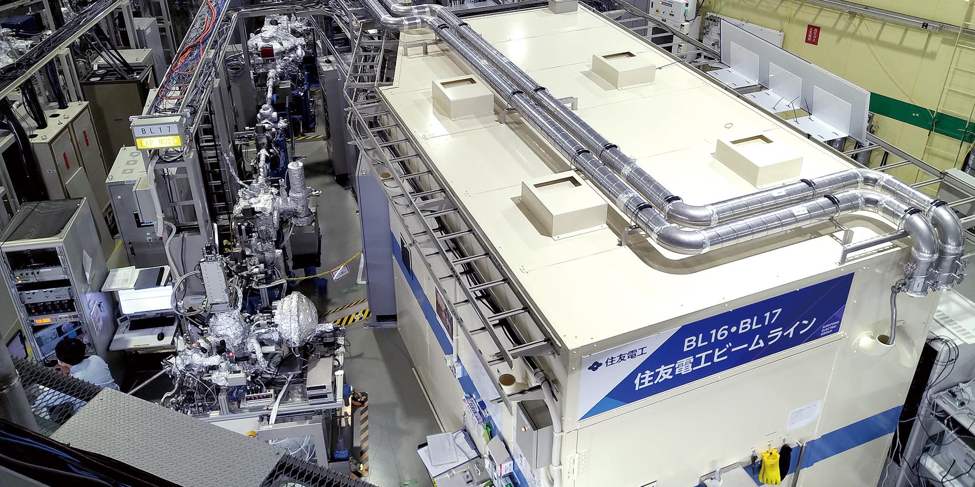
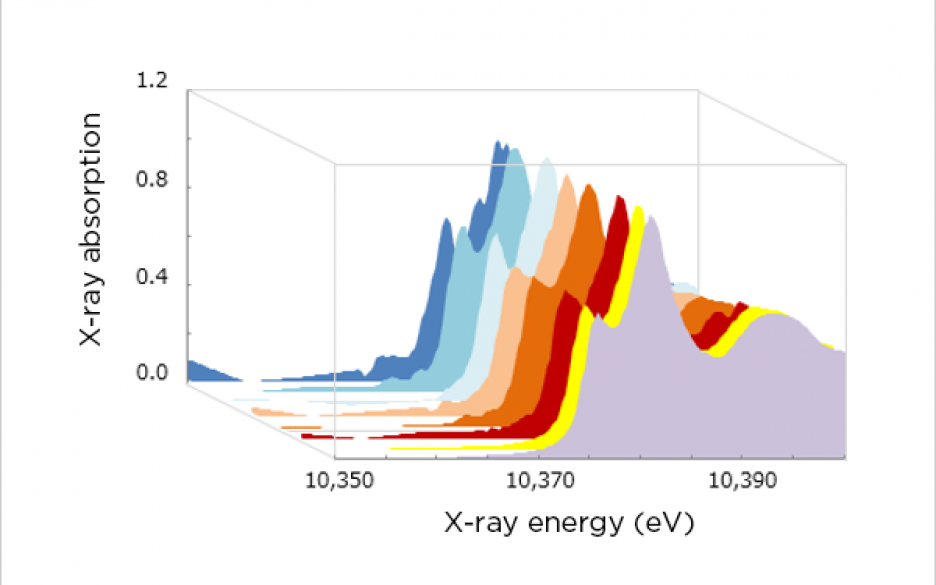
“One of our tasks is to probe into the cause of uneven quality. In the manufacturing process, some steps cause damage to gallium nitride, which is used as a material. Our mission is to explore the damage. For example, we evaluate and identify various types of damage to GaN, which is a compound of nitrogen (N) and gallium (Ga), such as differences in the composition, oxidization of the GaN surface, contamination with impurities, and defects of the crystal structure. Such damage results in deterioration of characteristics that GaN HEMTs are expected to offer. Thus, it is essential to probe into the cause. Based on the analysis results, the manufacturing sites optimize the process conditions to carry out kaizen and improve the quality. Analysis technologies also contribute to development activities to enhance the product performances. The Sumitomo Electric Beamline , which has been installed at the Kyushu Synchrotron Light Research Center in Tosu City, Saga Prefecture, is very useful in analyzing materials on an atomic level and help differentiate ourselves from competitors,” said Saito.
Synchrotron radiation and luminescence
— Establishing various analysis techniques
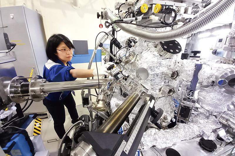
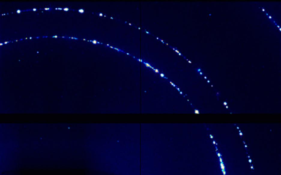
Synchrotron radiation, which was mentioned by Saito, is an extremely intense artificial beam that is generated by a large-scale accelerator. The beam consists of powerful, short-wavelength electromagnetic waves (X-rays) that get emitted when the path of high-speed electrons is bent by a magnet. Irradiating a material with these X-rays causes the release of various signals from the material. By studying these signals, the structure and characteristics of the material can be analyzed on an atomic level. In the synchrotron radiation experiment facilities, we can perform in-depth analytics by using high-strength X-rays 10,000 times to 100 million times more intense than those of small equipment. The Sumitomo Electric Group started its synchrotron analysis activities at public beamlines at SPring-8 in Hyogo Prefecture, which is one of the largest synchrotron radiation facilities in the world. Then, it installed its own beamlines at the Kyushu Synchrotron Light Research Center in Tosu City. These beamlines have been operated since November 2016 to meet various analysis needs, including devices. Takumi Yonemura of the Yokohama Analysis Dept. was engaged in synchrotron radiation analysis for some time after he joined the company. At present, Yonemura works on an analysis technique called photoluminescence to use synchrotron radiation more effectively.

“In photoluminescence, a substance or material is irradiated with a laser beam to observe the photons, which are generated when the excited electrons return to their ground state. The generated photons are easily affected by defects and impurities in a substance. Thus, in-depth analysis of the obtained emission spectrum makes it possible to acquire information about defects and impurities in the substance. This is one of the techniques to evaluate the process damage for GaN HEMTs. Based on the information about defects derived from photoluminescence, we determine the defect and find out how it affects the product characteristics by using synchrotron radiation and scanning transmission electron microscopy. In developing analytics and analysis techniques, it is important to collaborate closely with the manufacturing team to identify product issues a few years ahead, introduce new analysis techniques that are required to solve issues, and develop analysis technologies in advance. I believe that such efforts help ensure good quality in the manufacturing operations,” said Yonemura.

Strong collaboration between development and manufacturing members and the ATRC
GaN HEMTs are developed and manufactured by Sumitomo Electric Device Innovations, Inc. Saito and Yonemura work in strong collaboration with the engineering staff of Sumitomo Electric Device Innovations. Shinya Nishiyama of the Quality Assurance Dept. is one of the engineering staff members. Nishiyama is responsible for verifying, evaluating, and assuring the quality of products to be shipped, in addition to those to be commercialized in the future.
“We have acquired a lot of findings about GaN HEMTs over many years of operations, so we regard them as mature products. However, some defects arise and cause problems in the process, which consists of many steps. The ATRC gives us reassurance when we need to cope with problems. We have maintained strong trusting relationships with customers thanks largely to the ATRC. We have been rapidly increasing production in response to the support in the market. We aim to enhance collaboration with the ATRC to market high-performance and high-quality GaN HEMTs,” said Nishiyama.
At present, further die shrink is required for GaN HEMTs to cope with the 5G high-frequency bands. It is also required to achieve higher output than before. To maintain market competitiveness, it is necessary to ensure high mass productivity and cost advantage. The ATRC has a key role to play toward further evolution of GaN HEMTs.

NEXT
Challenges Toward “CASE” Innovation in the Auto Industry
-Evaluating the reliability of wire harnesses and designing high-speed communication parts-
Registration of public notification
If you register your e-mail address, we will notify you when the latest issue is published. If you wish, please register from the registration form.
To delete your registration, please visit here.