07 July 2025
Sumitomo Electric Elucidates Electron Scattering Mechanism in Heterojunctions of Novel Nitride Semiconductors —Improved Performance of GaN-HEMTs Paves the Way for Advances in Next-Generation High-Frequency Communications Technology—
Sumitomo Electric Industries, Ltd., through joint research with the research group led by Assistant Professor Takuya Maeda at the University of Tokyo (Location: Bunkyo-ku, Tokyo; President: Teruo Fujii; hereinafter referred to as "the University of Tokyo"), has discovered the scattering mechanism of two-dimensional electron gas in the heterojunction*1 of scandium aluminum nitride (ScAlN) and gallium nitride (GaN), which is a strong candidate of the barrier layer of next-generation high-frequency GaN high electron mobility transistors (GaN-HEMTs).
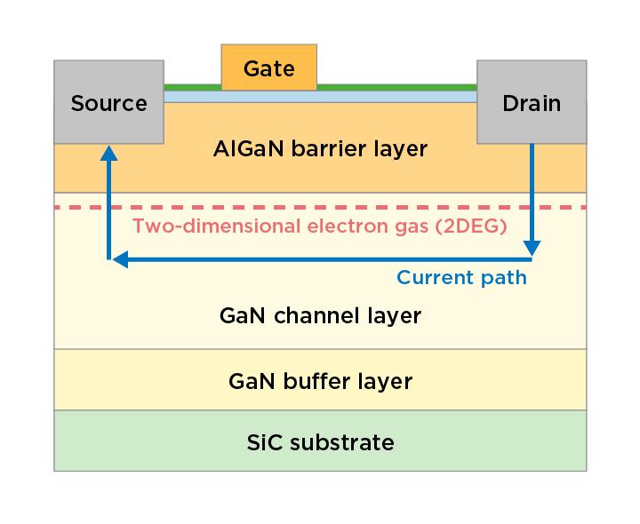
In the structure of commonly used GaN-HEMTs for high-frequency applications, GaN crystals are grown on a silicon carbide (SiC) substrate, and a heterojunction of grown aluminum gallium nitride (AlGaN) is formed on top of the GaN crystal to create a two-dimensional electron gas (2DEG) on the interface, through which electrons move at high speed. ScAlN, which has a high electron generation capability, is attracting attention as a next-generation barrier layer to develop higher frequency and higher power GaN-HEMTs.
So far, the heterojunction between ScAlN and GaN has attracted a high density of electrons, but its mobility is limited by some kind of scattering factors. The limiting factor of the mobility has not been understood. This study revealed that the mobility of 2DEG in ScAlN/GaN heterostructure is mainly limited by interfacial roughness scattering*2.
Role of the joint research
Sumitomo Electric:
Provision of high-quality GaN/SiC substrates for research
The University of Tokyo:
Fabrication of ScAlN/GaN heterojunctions on GaN/SiC substrates, measurement and analysis
The results of this research received high praise at the International Conference on Nitride Semiconductors (ICNS), the largest international conference in the field of nitride semiconductors, and we were invited to give a presentation.
Moving forward, we hope to improve the interfacial roughness and achieve high-density and high-mobility 2DEG formation to enhance the performance of GaN-HEMTs used in next-generation high-frequency communications, and also to apply this technology in our GaN-HEMTs.
For more information, please see the University of Tokyo press release.
*1 heterojunction:
A junction formed by the combination of different semiconductor materials.
*2 Interfacial roughness scattering:
A phenomenon in which irregularities at the interface of a heterojunction impede the transfer of electrons.