Revolutionary Devices for High-Speed and Large-Capacity Communication
History of development of GaN HEMTs ②

Development of new devices by applying the working principle of HEMTs
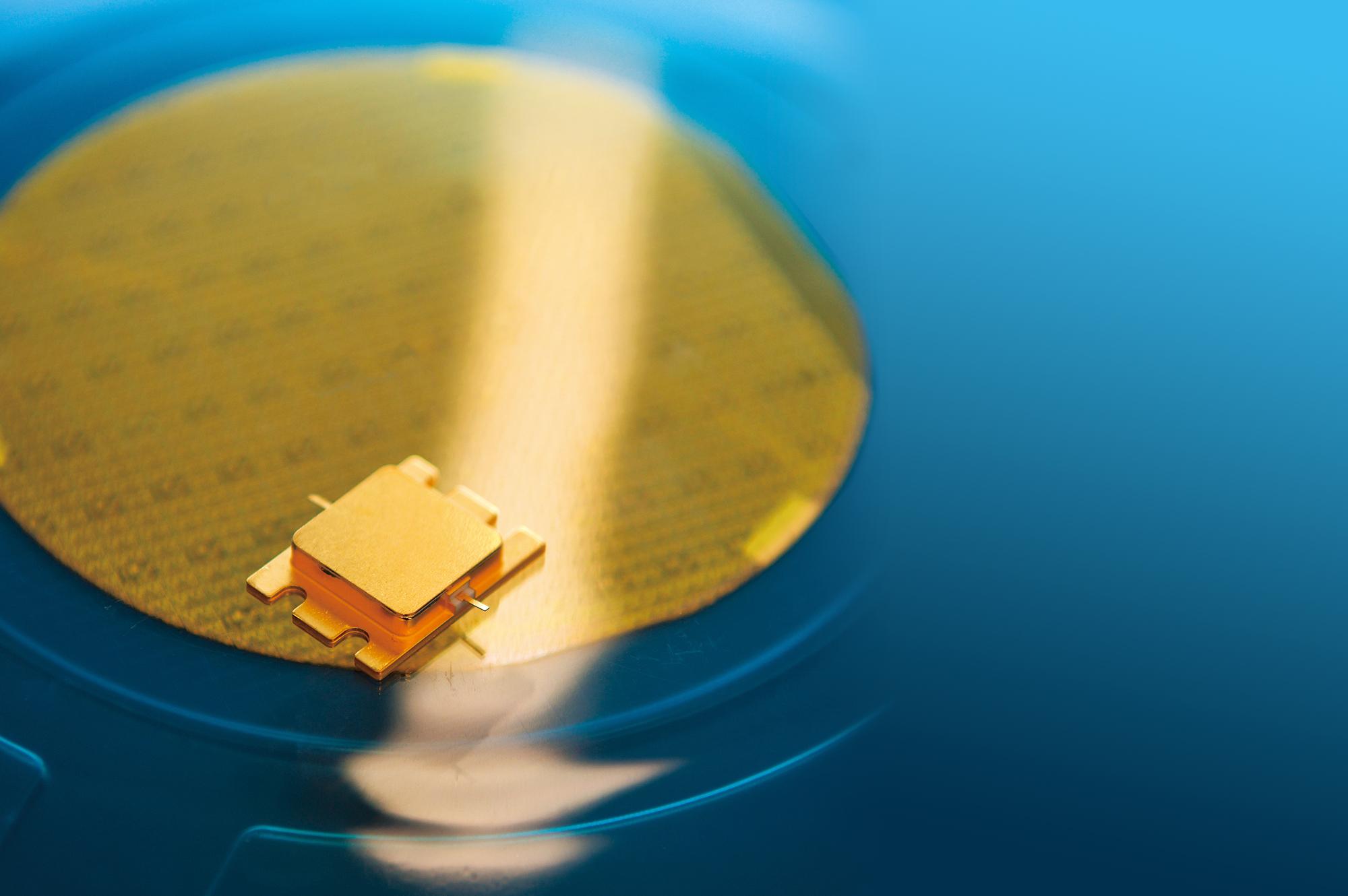
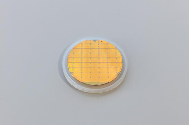
GaN HEMTs were developed based on the concept of HEMTs, which used a spatially separated double-layer structure (i.e., an electron generation region and an electron transport region) in a transistor. Aluminum gallium nitride (AlGaN) was used in the electron generation layer, and GaN was used in the electron transport layer. Silicon carbide (SiC), which is used for the substrate, is characterized by excellent thermal conductivity. This structure efficiently radiates the heat generated when a transistor is operated. A monocrystalline film of GaN and AlGaN each is allowed to grow on the SiC substrate using a technology called epitaxy. Finally, electrodes are formed. This is how GaN HEMTs are manufactured.
The first issue was that SiC was expensive and hardly available. It was difficult to set the optimal condition for the growth of monocrystalline films by epitaxy. Even after resolving these issues, it was extremely difficult to ensure reliability. The voltage resistance was high, but GaN HEMTs broke down easily when voltage was applied for energization and operation. Investigation of the cause revealed a quality problem in the SiC that was used for the substrate. Further efforts were made to ensure reliability by improving the quality of the substrate in close cooperation with the SiC substrate manufacturer. Fumikazu Yamaki was one of the members who worked hard to deliver GaN HEMTs. He is currently in charge of design and development of transistors at Electron Device Development Dept., #1 of SEDI.

“We had to improve the poor yield. To sell novel products to customers, we had to offer products of reliable quality. We continued to work to find the cause of the defects. To identify and remove defective products, we developed a proprietary screening technology and established a screening method. Instead of simply manufacturing products, we consistently placed top priority on quality,” recalls Yamaki.
To ensure reliability for customers
While concerted efforts were made to clear hurdles in the development of GaN HEMTs, a sales campaign was launched to raise the profile and awareness of GaN HEMTs by offering samples. Nobuhiro Kuwata, who is currently the president of Sumitomo Electric Asia, Ltd. in (Hong Kong), was one of the sales members in charge.

“Only users could experience the extremely high characteristics demonstrated by GaN HEMTs. We promoted a campaign, in which we asked many customers to let their engineers conduct measurements using the actual samples and helped them deepen their understanding about GaN HEMTs. GaN HEMTs demonstrate their advantage at 50 V, however, no base stations of that time had power supply units operated at that high voltage. Therefore, we asked a power supply unit manufacturer to develop and commercialize a 50 V power supply unit. While setting up the environment in which GaN HEMTs could demonstrate their performance to the fullest, we promoted sales activities toward commercialization.
The key was in the introduction of a digital distortion compensation technology, which eliminates distortion of input signals in amplifiers at base stations, and guarantees the communication quality and operation with low power consumption. At that time, digital distortion compensators were optimized for Si-LDMOSs, so we had to present examples of distortion compensation measurement for the GaN characteristics by ourselves. These efforts helped customers gradually understand the characteristics and advantages of GaN HEMTs,” recalls Kuwata.
Kuwata and other members were engaged in awareness-raising and sales activities not only in Japan but also in North America, Europe and Asia. They kept in mind the supply of GaN HEMTs to the global market from the outset. Shipment of samples began in 2005, and mass production started in 2006. In Japan, GaN HEMTs were chosen for 3G base stations in 2007. SEDI became the first company in the world to commercialize GaN HEMTs.
In the initial stage of development of GaN HEMTs, the development, manufacturing and sales departments of SEDI worked as a unified team instead of working separately.
“All the members shared the chagrin of defeat by Si-LDMOSs and a wish to turn the tables by marketing GaN HEMTs as devices for base stations,” says Kuwata.
SEDI succeeded in delivering the world’s first product, but issues remained unresolved. The yield improved, but the high price was inevitable. In Japan, there was a growing awareness about GaN HEMTs’ outstanding operation with low power consumption, and GaN HEMTs were increasingly used by customers. However, Si-LDMOSs (which were competitors) remained dominant in the global market. The shipment volume did not readily increase. Under these circumstances, the SEDI engineers worked to cut costs extensively.

NEXT
From the First Year of 5G to “Beyond 5G”
Current developments of GaN HEMTs that continue to evolve
Registration of public notification
If you register your e-mail address, we will notify you when the latest issue is published. If you wish, please register from the registration form.
To delete your registration, please visit here.