Revolutionary Devices for High-Speed and Large-Capacity Communication
History of development of GaN HEMTs ①
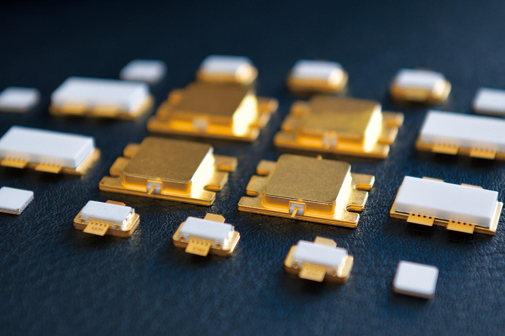
What are HEMTs?
GaN HEMTs are electronic devices that underpin the era of 5G. Before going into the details of GaN HEMTs, it is necessary to explain HEMTs, which are an outstanding accomplishment derived from Japan’s high engineering capability and researchers’ tremendous creativity. The technology was developed in Japan and gave a strong impetus to the progress of telecommunications technology.
HEMT is the abbreviation for high-electron-mobility transistor. As the name indicates, an HEMT is a type of transistor. The transistor was invented by Bell Laboratories (in the U.S.) in 1948 and had the greatest impact ever in the world of technology. It heralded the beginning of the era of electronics. In fact, transistors are devices that laid the foundation for rapid development of electronic technologies, including computers. One of the functions of transistors is amplification to increase the signal strength. For example, a transistor radio incorporates a transistor that amplifies weak signals transmitted through the air to drive the speaker.

At first, transistors were manufactured using germanium. Eventually, germanium was mostly replaced by highly heat-resistant silicon. In the 1970s, a project was launched in Japan to improve transistors. Researchers focused on the speed of electrons. Conventional silicon transistors incorporated an electron generation layer and an electron transport layer in the same material. For this reason, the speed of electrons was reduced when electrons collided against impurities. To solve the problem, a HEMT was developed using a compound semiconductor by Fujitsu Laboratories Ltd. in 1979. A double layer structure was employed. An electron generation layer made of aluminum gallium arsenide (AlGaAs) crystals was placed on top of an electron transport layer made of high-purity GaAs. This device structure achieved high-speed and high-sensitivity processing of electric signals. In 1985, HEMTs were first used in satellite broadcasting receivers in many countries. They have become devices indispensable for various apparatuses in the microwave and millimeter-wave ranges, such as mobile phones and base stations, satellite navigation receivers, and millimeter-wave radar sensors for preventing collision of vehicles. To date, HEMTs have served as the fundamental technology underpinning the telecommunications society. GaN HEMTs were developed by combining the technological achievement of HEMTs with GaN, characterized by superior material properties. Sumitomo Electric Device Innovations, Inc. (SEDI) led the development and manufacturing.
Challenges to harness the potential of gallium nitride
For 1G analog mobile phones, silicon was used as the semiconductor material of high-output transistors (i.e., amplifiers at mobile phone base stations). For 2G in the first half of the 1990s, when digitalization started, the Sumitomo Electric Group was well prepared to market GaAs field effect transistors (FETs) in a timely manner. GaAs FETs attracted much public attention because these transistors allowed electrons to travel at a speed nearly five times that of silicon transistors and reduced power consumption. However, silicon laterally diffused metal–oxide–semiconductors (Si-LDMOSs), which were newly marketed transistors, had an advantage over GaAs FETs in all aspects, including characteristics and price, and dominated the market to drive 3G. The electronic devices sold by the Sumitomo Electric Group were completely expelled from the market. SEDI President & CEO Yuichi Hasegawa called it a “defeat.”
“GaAs FETs were defeated by Si-LDMOSs in the market competition. We faced a difficult situation, where business continuity came into question. Under such a critical situation, we were informed about a new compound semiconductor, for which a basic development project was underway at our laboratory. It was GaN. The characteristics were superior to those of silicon and GaAs. GaN was expected to be applied to electronic devices to achieve high output and high speed. We had no choice but to commit ourselves to GaN in a do-or-die effort,” recalls Hasegawa.
In 2000, the engineering team of SEDI started the development of GaN HEMTs with the future potential of GaN in mind. Masahiro Nishi, who is currently affiliated with the Device Manufacturing Engineering Dept. of SEDI, was one of the development members.

“In terms of the material properties of GaN, we were impressed by the high breakdown voltage (breakdown field strength), which was about 10 times that of silicon. The saturated electron velocity, which represents the maximum speed of electrons when voltage is applied gradually, was twice or more that of silicon. The characteristics of GaN were expected to enable high-voltage operation, attain high efficiency, reduce power consumption, and achieve high output. We thought that GaN had the potential to offer devices that could match Si-LDMOSs,” says Nishi.
At that time, Kazutaka Inoue, who is currently the Department Head of the Device Process Development Dept. of SEDI, was struggling to revive the GaAs transistors.

“We were planning to regain our market share, which had been dominated by Si-LDMOSs, by thoroughly investigating the structure of GaAs and creating a new transistor that took full advantage of the characteristics. The thorough investigation made it possible to know the limits of GaAs’s performance. That is why we joined the development of GaN, but it was unknown territory for everyone. We had to start from scratch and tread a thorny path,” recalls Inoue.

NEXT
Revolutionary Devices for High-Speed and Large-Capacity Communication
History of development of GaN HEMTs ②
Registration of public notification
If you register your e-mail address, we will notify you when the latest issue is published. If you wish, please register from the registration form.
To delete your registration, please visit here.