Transmission Devices Laboratory
Our unique technology encompasses semiconductor crystal growth, epitaxy, processing, high-precision assembly of optical and electronic devices, and optical transceiver design. Using the complete spectrum of technology we possess, we are developing advanced compound semiconductor materials and related products for two major communications markets, that is, optics and wireless. We also aim to enter the non-communications market employing our cultivated elemental technologies.
Compound Semiconductors and their Applications
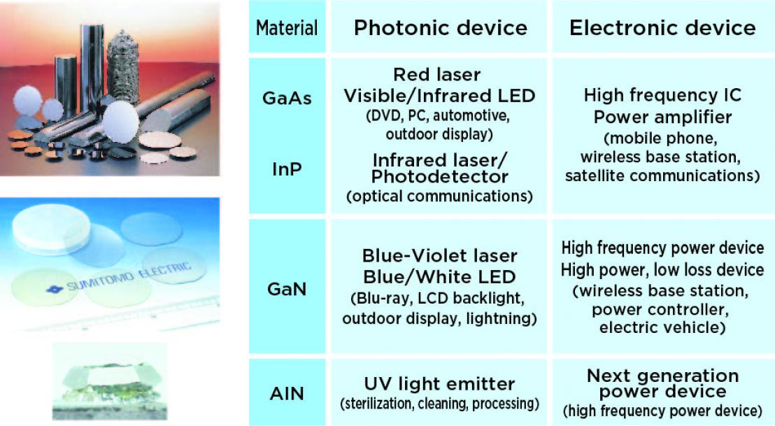
We are a pioneer in compound semiconductors, which are applied to various products where silicon cannot be used. We have commercialized a wide array of materials, and are now developing a crystal growth process with higher quality and a larger diameter as well as new materials for cutting-edge electronic devices.
* Blu-ray is a trademark or registered trademark of Blu-ray Disc Association.
Optical Device
We are developing semiconductor devices for optical-electrical signal conversion in optical communications systems.
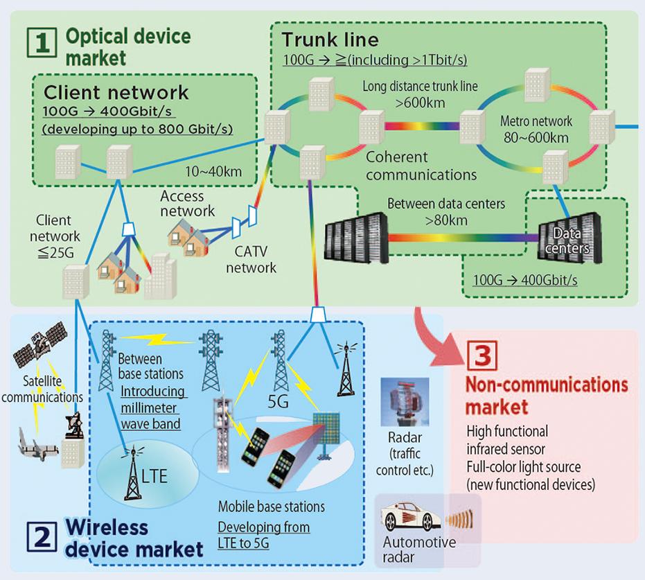
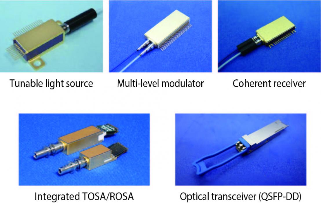
In trunk lines, digital coherent technology is used to realize 10 Tbit/s-class ultra-high capacity transmission. As key components, we are developing high-power tunable narrow-linewidth light sources, multi-level modulators, and coherent receivers employing our compound semiconductor technologies.
For client networks and data centers, we are developing optical subassemblies (OSA) and higher data rate optical transceivers. To cope with the rapid growth of optical network capacity, we are tackling miniaturizing and energy-saving technologies as well as higher transmission speed.
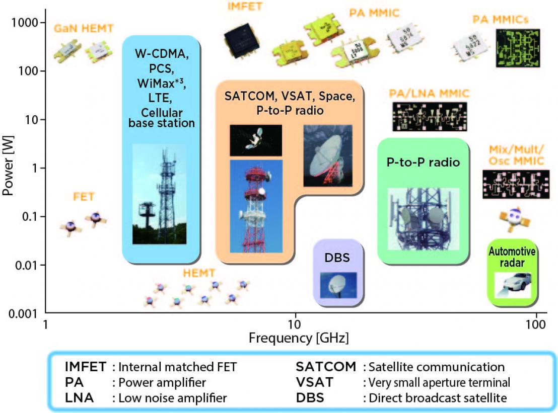
Wireless Device
We developed gallium arsenide (GaAs) HEMTs*1 ahead of our competitors and have supported the expansion of wireless communications. Applying this technology to gallium nitride (GaN), we have greatly contributed to the miniaturization and higher efficiency of high-speed mobile communications (LTE) base stations.
In addition, for the introduction of next generation 5G networks, we aim to create advanced devices with higher frequency and higher efficiency. Using high power and high efficiency features, we are pushing ahead with applications for larger communications capacity among base stations and satellites as well as solid state radar. HEMTs are integrated into MMICs*2, which are used in millimeter wave automotive radar.
*1 HEMT: High Electron Mobility Transistor
*2 MMIC: Monolithic Microwave Integrated Circuit
*3 WiMax is a trademark or registered trademark of WiMax
Ultracompact RGB Laser Module
We are developing ultracompact RGB laser modules combining our visible laser diode technologies as well as precision assembling processes for transmission devices. Semiconductor light sources of the three primary colors: red, green and blue, are integrated with optical components and thermoelectric coolers which enable effective temperature control and stable laser oscillation. We have achieved clear projected images using our laser alignment technique for the three primary colors.
Wide application to head-up displays, projectors, pointers, illuminators, and other industrial equipment is promising.
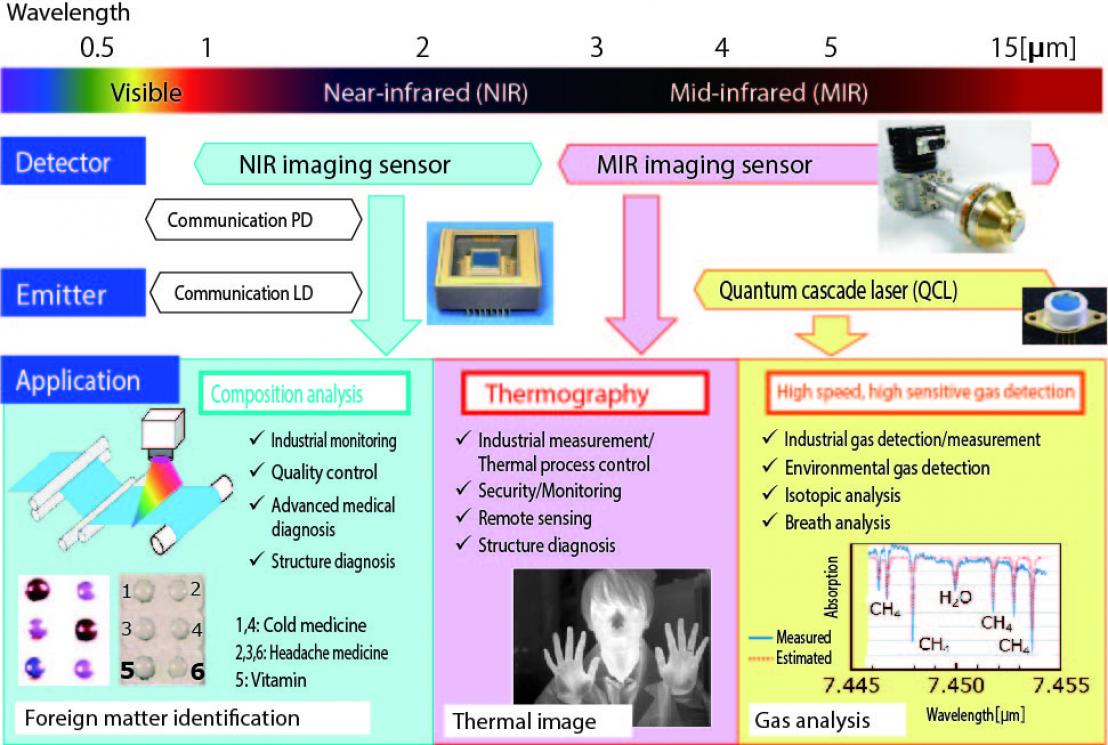
Infrared Sensing Device
We are developing quantum well infrared imaging sensors using elemental technologies from photodetectors for optical communications. With higher sensitivity, our sensors are suitable for microanalysis equipment and diagnosis systems which can visualize slight temperature differences. We are also conducting R&D in mid-infrared quantum cascade lasers for highly sensitive gas detection.