Advancing the Smart Society with Heterogeneous Material Integrated Optical Devices

Low Power Consumption Tunable Lasers with Heterogeneous Material Integration
Dr. Takuo Hiratani
Assistant Manager, Transmission Devices Laboratory
With the proliferation of IoT technology, which connects things to the Internet, a smart society is becoming a reality with automated driving and telemedicine facilitated. This trend greatly improves the quality of our lives. Consequently, the demand for data transmission grows every year and is expected to surge tenfold by 2030. As the required transmission capacity cannot be met using conventional single optical transceivers, multi-channel systems are being developed. However, this shift brings a considerable increase in power consumption, revealing limitations in conventional technologies. To overcome this challenge, we have focused on heterogeneous material integration, which generates synergistic effects through the combination of different materials. A new wavelength-tunable laser, which is an essential component in optical communications, has been developed using this approach. Our prototype demonstrates stable operation over a broad range of wavelengths and cuts down power consumption, a significant progress toward a smart society.
Revolutionizing Optical Devices with Heterogeneous Material Integration
Semiconductor materials commonly used in optical communication devices include Group III-V compound semiconductors and silicon. Group III-V compound semiconductors, comprised of elements from Groups III and V of the periodic table, are valued for their emission properties and used in light sources, high-speed and high-efficiency modulators and photodetectors. Silicon, on the other hand, offers ease of processing. Devices built from silicon photonics result in the miniaturization of devices via high-density integration and cost cuts facilitated by the use of large-diameter wafers. Both materials play significant roles in telecommunication infrastructures and data centers.
However, these optical devices are generally fabricated with a single material, and device performance is reaching its limits. Supporting future high-speed and high-capacity transmission with conventional single-material optical devices necessitates the use of a number of optical devices, posing a major challenge to energy and space conservation.
To overcome this challenge, we have focused heterogeneous material integration, which combines the benefits of Group III-V compound semiconductor devices and silicon photonics devices.
Experimenting with Heterogeneous Material Integrated Wavelength Tunable Lasers
As an initial step, we fabricated a prototype of a wavelength tunable laser by integrating heterogeneous materials. This laser, vital to wavelength-multiplexing optical communications, can alter light wavelengths. Its manufacturing process involves bonding wafers of different materials and processing semiconductors. For the bonding process, we bonded a Group III-V compound semiconductor wafer, which has crystals for light emission as the gain region, onto a silicon photonics wafer, which consists of a light-propagating optical waveguide, a light-reflecting loop mirror, and a ring resonator that permits only light at a particular wavelength to pass. This technique enabled higher density integration and lower coupling loss than other approaches.
The semiconductor is then processed to facilitate a seamless, minimal-loss junction between the gain region and the silicon photonic circuit via a two-stage tapered waveguide. This structure, comprising two gradually expanding tapers, enables a gradual light shape transformation while minimizing coupling loss of distinct material and shape waveguides. The tapers are positioned between the gain region and the silicon optical circuit to connect each other. This innovation not only manages to reduce the coupling loss, but also maintains stable optical output across a wide wavelength range, thereby ensuring stable operation.
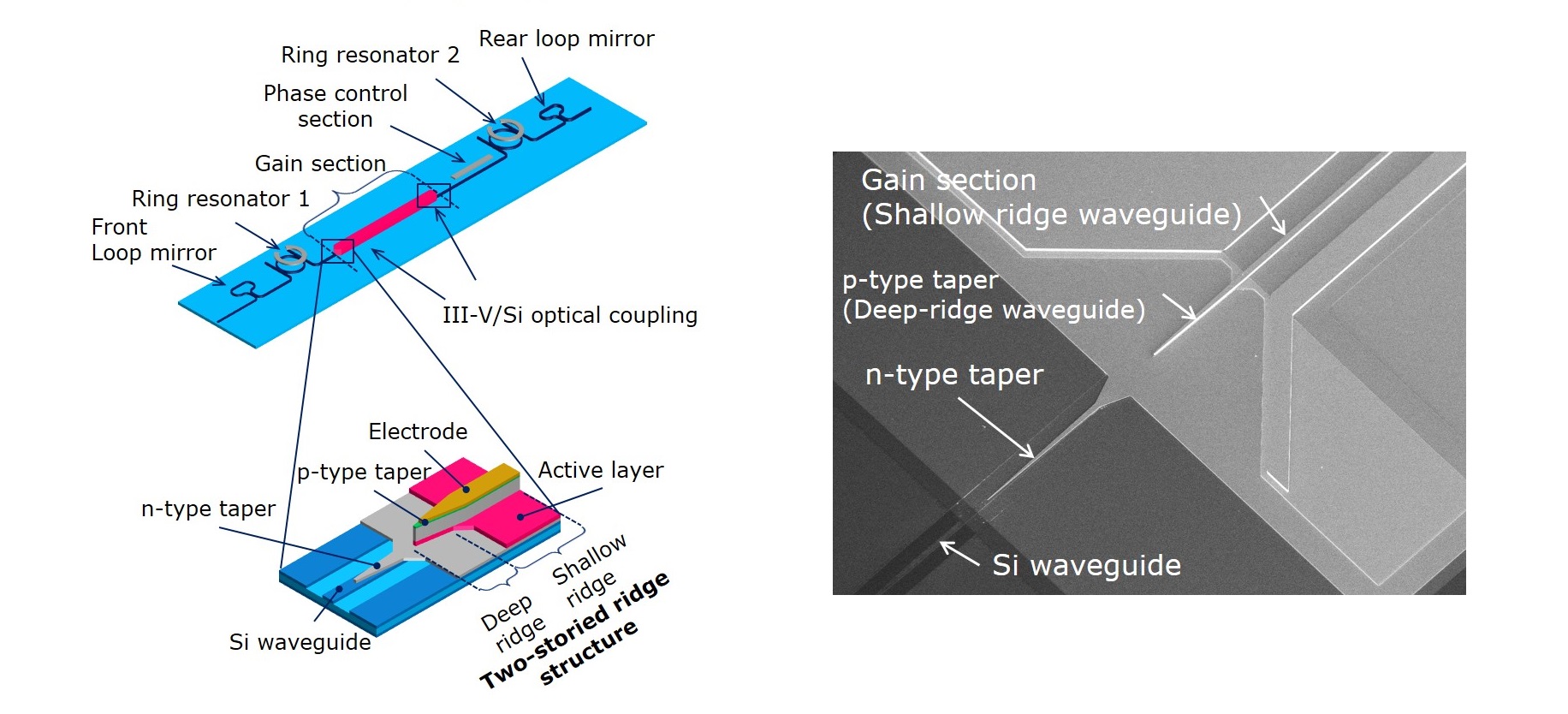
Overview of an InP/Si hybrid tunable laser using wafer bonding and InP/Si optical coupling structure
Envisioning a Smart Society
To address the rising demand for data transmission, we have explored optical devices that integrate Group III-V compound semiconductor devices with silicon photonics devices. The prototype wavelength tunable laser integrated with heterogeneous materials has confirmed high wavelength tunability and low power consumption.
We are already working on the next step by investigating compact optical devices that integrate various functional elements on a single chip. Currently, collaborations within and outside the Company, including joint research with universities, are supporting our activities. We will continue to steadily advance our research and development, solving problems one by one, so that our technology can contribute to the realization of a prosperous smart society.
 With senior colleagues
Related Information
[Paper] T. Hiratani, N. Fujiwara, T. Kikuchi, N. Inoue, T. Ishikawa, T. Nitta, M. Eissa, Y. Oiso, N. Nishiyama, and H. Yagi, "III-V Gain region/ Si external cavity hybrid tunable lasers with InP-based two-storied ridge structure," ISLC 2021, paper TuA3-6 (2021).
[Paper] T. Kikuchi, T. Hiratani, N. Fujiwara, N. Inoue, T. Nitta, M. Eissa, T. Mitarai, Y. Wang, Y. Oiso, N. Nishiyama, and H. Yagi, "III-V gain region/Si waveguide hybrid lasers with InP-based two storied ridge structure by direct bonding technology," Jpn. 052002-1-10 (2022).


SUMITOMO ELECTRIC TECHNICAL REVIEW
A journal of technical papers explaining the Sumitomo Electric’s technologies. Technical papers are available in PDF format.
Learn more