

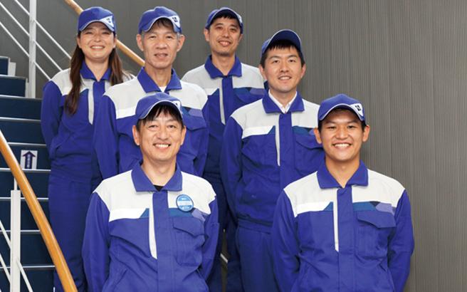
Many of the improvements I made are the result of teamwork
“It is certain that the era of optical communication using next-generation InP (indium phosphide) semiconductors will come. It will be absolutely interesting to work on this new technology because it is not yet on the market.”
This is advice I received from my older brother who conducted research on InP when he was in university. Convinced by this advice, I joined Sumitomo Electric and requested to be assigned to a department involved in InP, a compound semiconductor, and was assigned to the Compound Semiconductor Materials Division. Compound semiconductors, which are used in a wide variety of products from familiar smartphones and automobiles to industrial machines, are indispensable to our daily lives. A wafer, which is a substrate of compound semiconductors, is made by thinly slicing a cylindrical mass (ingot) formed by growing a crystal of the material. Since joining Sumitomo Electric Industries, I have been involved in slicing, including the setting up of new cutting equipment and the development of slicing processes for special products.
Since compounds handled in the slicing process are expensive, it is important to minimize losses and stably obtain as many wafers (substrates) as possible from a mass of material. When I was young, I worked with the help of my supervisors, seniors, and technical staff, and when purchasing wires, I negotiated with suppliers’ engineers as well as their sales staff to collect as much information as possible. Then, while using the information obtained in this way as reference, I processed many samples, analyzed data, and repeated the PDCA* cycle to master the characteristics of equipment and materials.
There was an unforgettable event when we were required to improve the accuracy of the InP slicing angle. The equipment we were using at that time could not achieve the desired accuracy. So, I devised a solution that could be realized by introducing new equipment and improving the process, and strongly requested the plant manager to let me implement it. Although my plan required a very large investment, the plant manager called the manufacturer of the necessary equipment the next day and decided to introduce it.
At first, I struggled alone because I was not able to achieve the accuracy I expected, but as a result of sharing the ideal work process with my team members and making improvements by thoroughly resolving the causes of problems one by one, I finally achieved the desired accuracy. This experience made me realize that cooperation with colleagues is a key to success in everything I do. It convinced me that we could improve our operation and maintain our high product quality by creating an environment where we can work hard as a team while closely communicating with each other.
* PDCA: An acronym for “plan,” “do,” “check,” and “act,” which represents a method to continuously improve management by repeating the cycle of these four steps.
Unforgettable words of my supervisor when I made a big mistake
The conditions and equipment for cutting compound semiconductors differ depending on the target product. We sometimes use a wire saw, a cutting device using a wire, which is required to be able to cut the material quickly, accurately, and stably according to the characteristics of the product. So, I informed a wire manufacturer of detailed wire requirements, thereby accomplishing the development of a technology to cut a new material with a thin wire, which had not yet been successful at that time. I also succeeded in developing a new slicing technology using the latest cutting equipment. Since these developments were highly evaluated for their contribution to the reduction of material loss and cost, in 2015, I was certified as an expert having important skills.
However, not all has been smooth sailing for me. I tried many developments to improve operations, and there were some failures. One of the most unforgettable failures was when I placed a special crystalline material on a cutting machine in the wrong way, which resulted in a large loss of valuable material that I had never made before. It was a mistake made by doing other work in parallel. I felt down and was fully expecting to be blamed by my supervisor, but he unexpectedly said: “I do not blame you for any mistakes that you make as a result of making proactive efforts. It would be rather a greater loss for the company if employees lose their willingness to make improvements because they are afraid of making a mistake. Continue to try to make improvements without being afraid of making a mistake.”
I still clearly remember these words and always keep them in mind when giving guidance to younger employees as an expert.
Professional pride and high goals
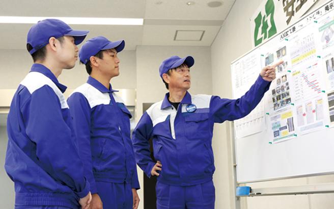
Partly because of these words of my supervisor, I do not blame younger employees when giving guidance to them. Even if they cannot do their tasks well, I thoroughly discuss with them until they find the causes and resolve them one by one. At that time, they need to share information in real time not only with site workers but also with other related persons, including engineering staff. When I see the process in which younger employees master a skill to such a degree that they can teach the skill to other employees and acquire professionalism, I feel a sense of accomplishment. Since each person has a different personality, it is important to understand it and give guidance in a way that suits the person. In this sense, I am being trained every day as an instructor.
Currently, I am involved in production, development for operational improvement, and the development of younger employees. The source of my energy is my willingness to accept challenges and my pride as a manufacturing professional. My motto is to profess my commitment to goals to motivate myself and make constant efforts to achieve them in cooperation with colleagues. Manufacturing cannot be done by an individual, but rather as a team, so relationships with colleagues are important. After preparing a suitable environment, I will continue to try to push the technical limits while flexibly responding to innovations that will take place across the world. I may face many obstacles in this process, but they will give me opportunities to improve my skills, so they are even kind of fun.
I am now working on the development of a new technology, which is expected to reduce our production cost and improve productivity. I believe that the accumulation of such improvements will lead to the development of our manufacturing sites.
PROFILE
Toshihiro Fujinaga
Advanced Material Section, Itami Plant, Manufacturing Department, Sumiden Semiconductor Materials Co., Ltd.
1990
Joined Sumitomo Electric Industries, Ltd. Assigned to the Slice Section,
Semiconductor Plant No. 2, Manufacturing Department, Compound Semiconductor Materials Division
2001
Leader of the Optical Slice Group, InP Section, Semiconductor Plant,
Manufacturing Department, Compound Semiconductor Materials Division
2006
Deputy Chief, Optical Processing Section, Itami Plant, Manufacturing Department, Sumiden Semiconductor Materials Co., Ltd.
2012
Chief, Processing Section, Itami Plant, Manufacturing Department,
Sumiden Semiconductor Materials Co., Ltd.
2014
Advanced Material Production Engineering Section, Engineering Department,
Sumiden Semiconductor Materials Co., Ltd.
2015
Certified as an expert (Slicing and outer surface processing of InP substrates and new materials): Still valid
2018
Chief, Advanced Material Section, Itami Plant, Manufacturing Department, Sumiden Semiconductor Materials Co., Ltd.