
24 years of experience in implementation of optical devices
Ever-evolving optical transceivers
The Yokohama Works that I work for was established as a development and manufacturing base of communication cables in the Kanto area. At present, it deals with information and communication-related products such as optical fibers and cables, optical connecters, fusion splicers, optical amplifiers, and optical and electronic devices. At first, I was assigned to the production site of power cables. There was a turning point in 1986, eight years after I joined the Company. A new device business was launched at the Yokohama Works, and I was engaged in manufacturing. In 1994, I was involved in R&D related to the implementation of optical devices to manufacture optical transceivers. However, I did not have any experience in this field, so I had to learn from scratch. I took on a new challenge, which was intriguing and exciting. Since then, I have worked on the development and implementation of optical devices for 24 years.
Optical transceivers are one of the priority optical products on which Sumitomo Electric focuses its resources to develop. Electric signals input into an optical transceiver are converted into optical signals on the transmission side, and optical signals are converted into electric signals on the reception side. This is a key device that determines the quality of optical communication. Optical transceivers have been improved continuously to reduce their size, power consumption and cost and increase the transmission speed to meet the needs for higher speed and larger capacity of optical communication. For example, we offer ultra-compact optical transceivers for 100 Gbit/s transmission. Optimal wire bonding between parts is an important technique to maximize the performance of these new products.
Craftsmanship of wire bonding
Requiring high precision of ±5㎛
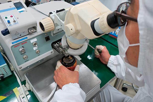
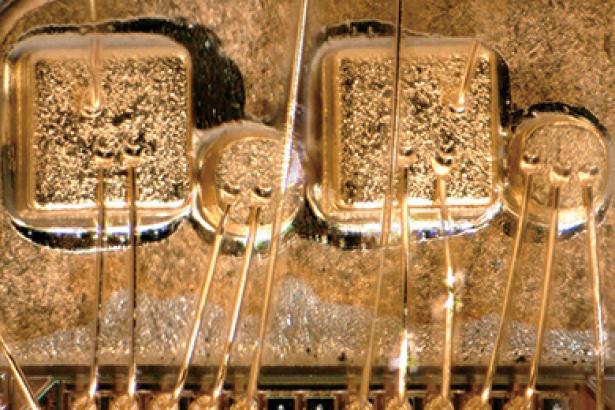
I am responsible for studying the possible wire bonding between parts and optimizing the layout of parts toward mass production of optical products such as optical transceivers. Wire bonding refers to a process to electrically connect an electrode on a circuit board with an electrode of an electronic part by using an ultra-fine wire of about 20 μm in diameter. The characteristics of parts are significantly affected by the wire length and the bond condition. Namely, wire bonding determines the performance of optical transceivers and the quality of communication. Obviously, wire bonding is performed based on a design drawing, but an automatic wire bonder cannot optimize the wire bonding while checking the characteristics of the parts that have been increasingly integrated and implemented in higher density. I connect ultra-fine wires with high precision within ±5 μm and study the feasibility of mass production based on my skills and knowledge that I acquired during 24 years of experience. The key point is to create the optimal shape for connection and minimize the wire resistance. In fact, this is a highly specialized skill.
Wire bonding is a versatile technique that is used for various applications such as connection between parts that are arranged on a flat surface, between parts that are arranged with a level difference or between parts that are some way apart from each other, as well as more difficult special connection methods such as ribbon wiring for high-frequency signals and stitch wiring between three electrodes. However, there is no well-established or standardized method. It is necessary to identify the peculiar characteristics of parts and equipment based on experience and to optimize wire bonding based on manual skills. The specifications for mass production are determined based on wire bonding and parts layout to market the products. This connecting a wire skill requires craftsmanship. It is an honor to have been certified as the only meister in the company for my advanced skills.


A mission to train younger engineers
A never-ending process to improve skills
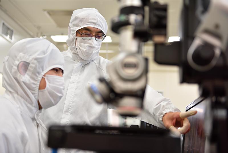
I have been certified as a meister not only for my skills but also for my commitment to training younger engineers, which is my important mission. As a trainer, I have passed on techniques to four engineers during the eight years since 2010 when I was certified as an expert. I will carry on this mission even after certification as a meister. Patience is the key to developing human resources. During training within a limited timeframe, I am often tempted to show how to perform wire bonding properly, but I must be patient not to do so. It is quite normal that trainees cannot do it right at first. Trainees should experience the process including mistakes. They can acquire skills only through experience. I am convinced that the efforts to share and pass on my skills to many engineers will directly result in high evaluation of our optical device products in the market.
Recently, I have been engaged in the development of a full-color laser module by taking full advantage of the technique that I have acquired. This product is being used as a projector light source of a robotic mobile phone. In my career as an engineer, I have had a new sense of satisfaction because I have been given an opportunity to deliver a product for general consumers. I assume that imagination and creativity are required because the technique to connect a wire is a manual skill. To achieve optimal wire bonding, I use imagination and creativity and work patiently without giving up until the last moment. That is my style of work. Improvement of skills is an endless process. My skills are not 100% perfect. I remain committed to acquiring more knowledge and brushing up on skills to attain higher goals as an engineer.

PROFILE
Akihiro Miura
1979
Joined Sumitomo Electric
Assigned to the Power Cable Group at the Yokohama Works
1986
In charge of the semiconductor process and manufacturing
Yokohama Research Div.
R&D Unit
1994
In charge of development of optical devices (to date)
Yokohama Administrative Section
Business Process Quality & Internal Control Promotion Dept.
R&D Group
2010
Certified as an expert
2018
Promoted to a meister

