
2013年1月号 No.182
特集「新しいエネルギー社会への貢献」

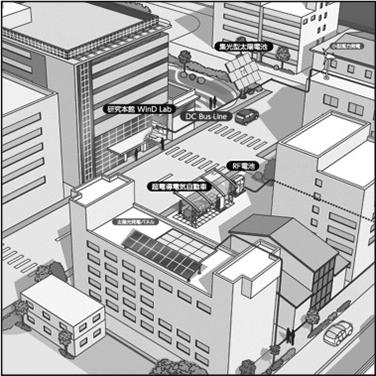
Sumitomo Electric Industries, Ltd. has recently developed two types of smart-grid demonstration systems. One is the micro smart-grid demonstration system operating at Osaka Works from June 2011. This system consists of four types of renewable power generators and a storage battery with DC-connection to balance fluctuations in natural power generation and power consumption, thereby ensuring stable and efficient power supply to the facilities and equipment of the Works without any commercial power
0.6 MB
0.6 MB
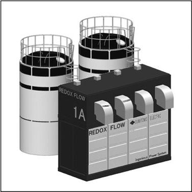
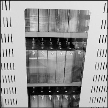
Renewable energies, such as solar and wind power, are increasingly being introduced as alternative energy sources on a global scale toward a low-carbon society. For the next generation power network, which uses a large number of these distributed power generation sources, energy storage technologies will be indispensable. Among these technologies, battery energy storage technology is considered to be most viable. Sumitomo Electric Industries, Ltd. has developed a redox flow battery system
5.3 MB
5.3 MB
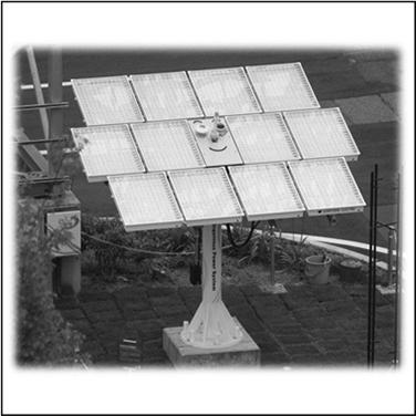
"Sumitomo Electric’s concentrator photovoltaic (CPV) system was developed under the design concepts of light weight, small size, good heat dissipation and use as a display. At its Yokohama Works, a megawatt-class generation and storage system was deployed for demonstration and has been in operation since July 2012. The performance of the CPV modules in this system was evaluated. The module recorded a conversion efficiency of approximately 30% both in sunlight and using a solar simulator.
0.5 MB
0.5 MB
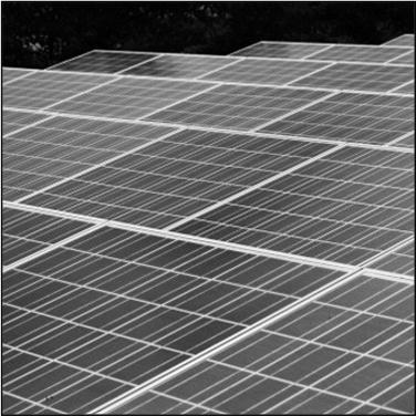
In Japan, an increasing number of megawatt-class solar power systems have been established for industrial use since the introduction of the Feed-in Tariff system, a policy that requires electric power companies to purchase electric power generated by solar power systems at a relatively high price. In line with this, we have added new functions to our 100 kW and 250 kW solar inverters with the aim of preventing voltage fluctuations that are caused by the increased number of solar power systems.
0.6 MB
0.6 MB
A molten salt electrolyte battery (MSB) is a sodium secondary battery that uses molten salt as its electrolyte and features high energy density and safety. Our molten salt has a melting point of 61˚C and needs to be heated to 90˚C for battery usage. As the battery has a high energy density (290 Wh/L) and requires no cooling space, small and lightweight battery systems become possible. Although lithium ion batteries (LIBs) and sodium sulfur (NAS) batteries are currently drawing attention for
1 MB
1 MB
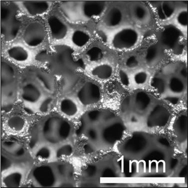
The authors have developed a novel porous metal “Aluminum-Celmet™” that is suitable for the cathode current collector of lithium ion batteries and other rechargeable batteries operated by high voltage. Aluminum-Celmet™ features a high porosity up to 98%, large relative surface area, unique threedimensional structure, and high corrosion resistance. In a demonstration test, the lithium ion battery using Aluminum-Celmet™ for its cathode current collector showed improved battery capacity,
0.4 MB
0.4 MB
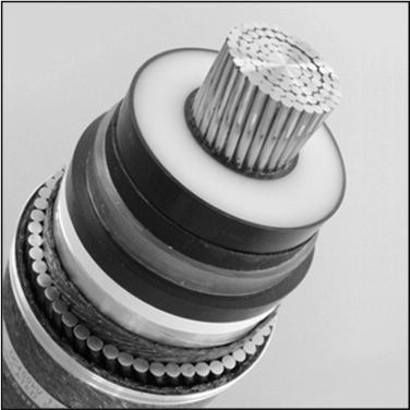
Japan’s first in-grid demonstration of a high-temperature superconducting (HTS) cable system has been started to evaluate its performance, safety and reliability. We developed the cable using the DI-BSCCO® HTS wire, and repeated design changes and element testing to meet required specifications. The performance of the cable was confirmed in the preliminary test using a 30-m HTS cable system and it was then successfully installed in Tokyo Electric Power Corporation’s Asahi Substation with
0.9 MB
0.9 MB
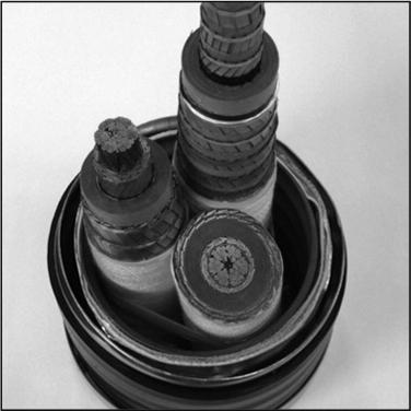
We have developed a DC-XLPE (cross-linked polyethylene) insulating material that has excellent properties for DC voltage applications. Our high-voltage DC-XLPE cable and factory joints using this material showed positive results in a long-term test partly consisting of a polarity reversal test at a rated voltage of up to 500 kV. In addition, this cable passed 250 kV pre-qualification tests and type tests, which also include polarity reversal tests, in accordance with the test conditions
0.7 MB
0.7 MB
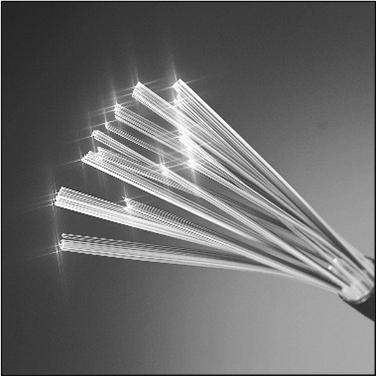
Optical fiber networks have expanded rapidly and more than 200 million km of optical fiber was sold in 2011. The optical fiber has now become a key technology to an information-oriented society. The conventional single mode fiber widely used in the world has not changed much in its refractive index profile, however, the coating materials and coating structures have developed due to changes in cable structures and installation environments. Coating materials play an important role in minimizing
0.9 MB
0.9 MB
As the electrification of automobiles progresses, hybrid electric vehicles have been in widespread use and the development of commercial electric vehicles has started. However, the heavy weight of these large vehicles leads to relatively short driving distances. To overcome this problem, the authors have been working on the development of high-efficiency motors using DI-BSCCO® hightemperature superconducting (HTS) wire. They have recently developed an HTS motor and conducted a demonstration
0.5 MB

0.5 MB
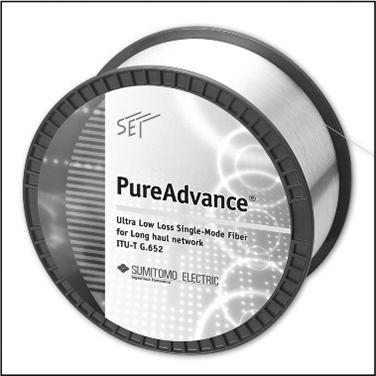
"To keep up with the exponential growth of demand for broadband Internet traffic, large capacity transmission systems with digital coherent technologies have started operation recently. The major challenge in such systems is to improve optical signal-to-noise ratio (OSNR). Although there would be several techniques to improve the OSNR, the use of low-loss and low-nonlinearity fibers would be one of the most straightforward and effective solutions. In this paper, we present newly-developed
0.5 MB
0.5 MB
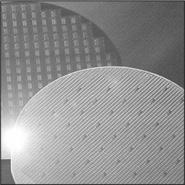
In the 3rd generation mobile communication systems such as W-CDMA, data traffic by cellular phones and other wireless tools has been steadily increasing. The data traffic is expected to further increase due to the wide spread use of smartphones and the introduction of WiMAX and LTE services that offer high-speed, high-capacity data transmission. A GaN (gallium nitride) HEMT (high electron mobility transistor) is suitable for the high-speed, highpower application owing to its excellent material
0.5 MB
0.5 MB
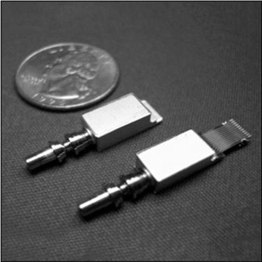
The authors have successfully developed a small receiver module with an integrated optical demultiplexer. The module is compliant with the 40GBASE-LR4 specification and sufficiently small (7 mm) to be mounted in a QSFP+ (Quad Small Formfactor Pluggable) next generation 40GE optical transceiver. The optical demultiplexer uses thin film band pass filters to divide a multiplexed optical signal into 4 demultiplexed optical signals, thereby realizing low optical insertion loss and low temperature
0.6 MB
0.6 MB
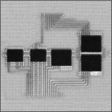
We have developed a transmitter chipset using a new tripler, up-converter, and power amplifier. Monolithic Microwave Integrated Circuits (MMICs) of these devices are designed using our Wafer Level Chip Size Package (WLCSP) technology, and reflow-soldered on a 10 mm x 14 mm printed circuit board (PCB). The WLCSP technology enables the development of highly integrated package-free flip-chip MMICs suitable for surface mounting, and is therefore expected to reduce the production cost significantly.
0.5 MB
0.5 MB
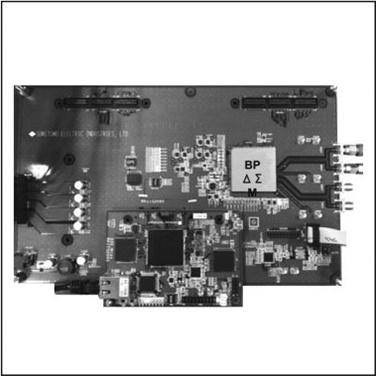
In wireless communication, there has been an increasing demand for high-speed and high-quality data transmission, particularly since the advent of smartphones. To meet these requirements, multipleinput and multiple-output (MIMO) systems and array antenna systems have been developed. Wireless systems are also increasingly being integrated for improved communication performance, while transmitters are required to remain compact. To this end, we have developed a 1-bit digital radio frequency (DRF)
0.8 MB
0.8 MB
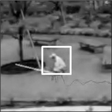
Information communication technology has been widely used for crime prevention and protection of the elderly. Currently, there is an increasing demand for video surveillance systems that can detect and report a stranger or suspicious behavior. Therefore, we have developed a video surveillance device that detects and tracks persons from the video sequence by using filtering logics and reports the result to the user through a network. This paper outlines the video surveillance device and its
0.5 MB
0.5 MB
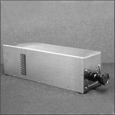
We have developed the Compovision® imaging system with a near-infrared (NIR) spectrographic camera. This camera incorporates a sensitive sensor that can detect the distinctive absorption spectra reflected or absorbed by organic substances in the wide wavelength band of 1,000-2,350 nm. The camera can process hyper-spectral data of 320 x 256 pixels at the frame rate of 1-320 fps, and thus enables precise real-time imaging. The Compovision® imaging system is expected to be used for the
0.6 MB
0.6 MB
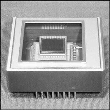
A twodimensional near infrared image sensor with the cut-off wavelength of 2.4 μm has been successfully developed by using InGaAs/GaAsSb type-II quantum well structures as its absorption layer. The 250-pair InGaAs (5 nm) / GaAsSb (5 nm) quantum well structures lattice-matched to InP substrates were grown by metal organic vapor phase epitaxy. The p-n junctions were formed in the absorption layer of each pixel by the selective diffusion of zinc. The sensor chip with 320 × 256 pixels at 30 μm
0.4 MB
0.4 MB