Forefront of Optical Device Research
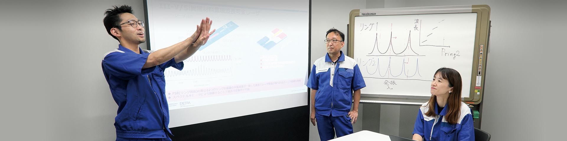
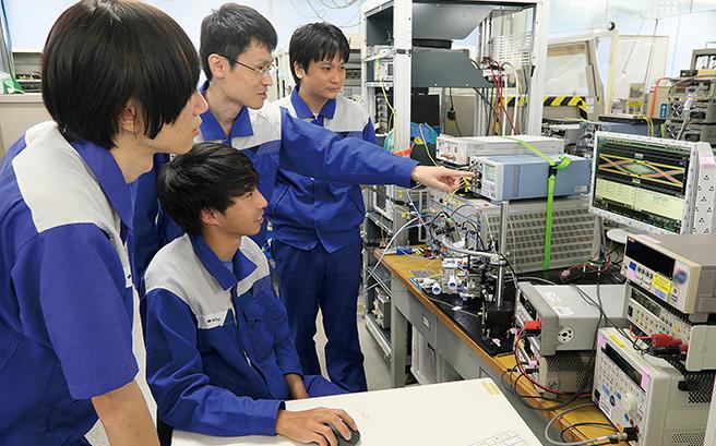
Research and development session (Design and discussion about next-generation lasers)
Heterogeneous Integration Technology and Photonic Crystal Surface-Emitting Laser
Indium Phosphide and Silicon Photonics
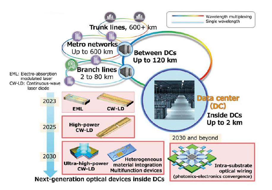
SEDI has been supplying high-speed, high-capacity optical devices with lower power consumption in response to market needs. Sumitomo Electric's Transmission Devices Laboratory has been at the forefront of this effort and has provided support. The transmission speed of optical communication is anticipated to reach around 10 Tbps in the 2030s. However, conventional single-material optical devices are showing limitations in high-speed operation; a technological breakthrough is necessary. To tackle this challenge, attention has turned to heterogeneous material integration technology. This technology involves combining and integrating components. Hideki Yagi, from the Optical Devices Department of the laboratory, has been actively engaged in cutting-edge research and development for many years.
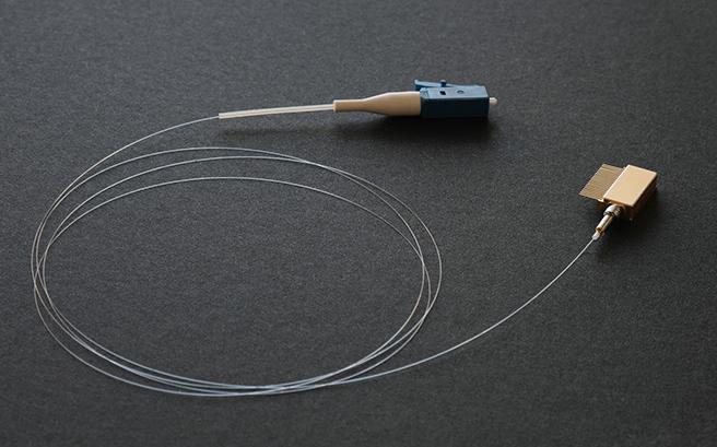
"Simply put, it is a technology that combines the advantages of indium phosphide semiconductors and silicon photonics.* An indium phosphide light source and a modulator are properly bonded to the silicon substrate that guides and controls light. This allows the compound semiconductor to achieve high speed, while silicon photonics enables miniaturization and low power consumption. We are currently developing a bonding technology that uses oxygen. To achieve this, we are keenly aware that we need to understand physical properties involved, as well as the knowledge and skills required for both silicon and indium phosphide processing. We aim to overcome this challenge and guide our efforts towards stable mass production." (Yagi)
*A technology that creates a waveguide on a silicon substrate to propagate and control light. Information is transmitted using optical signals instead of conventional electronic circuits (electrical signals).
Towards Game-Changing Photonics-Electronics Convergence Technology

Another major theme that the Transmission Devices Laboratory is addressing is "ultra-high output CW-LD." It is a next-generation semiconductor laser that uses a photonic crystal surface-emitting laser (PCSEL). This type of semiconductor laser emits light uniformly from the surface of the chip, achieving higher output compared to conventional semiconductor lasers that emit light from the edges. Masaki Yanagisawa, General Manager of the Optical Devices Department, is leading the research and development.
"When you increase the light-emitting area to achieve high output from a semiconductor laser, the beam quality tends to deteriorate. The PCSEL breaks through that limitation. By using a structure called a 'photonic crystal,' we can achieve high output without degrading the beam quality." (Yanagisawa)
The Transmission Devices Laboratory is currently addressing two major themes. What direction will future optical devices take?
"From the perspective of reducing environmental impact, the demand for lower power consumption in optical devices will always exist. In response to this demand, we have begun working on photonics-electronics convergence technology. This technology combines electronic and optical devices, replacing electrical wiring with optical wiring, aiming to increase network capacity, reduce latency, and achieve significant power consumption reduction. I want to develop technology and products that will have a positive impact on society and be a game-changer." (Yanagisawa)
NEXT
Leading Sales Strategies for the AI Era
- Sumitomo Electric Group's Optical Devices Are Being Deployed in Collaboration with Overseas Sales Offices -

Registration of public notification
If you register your e-mail address, we will notify you when the latest issue is published. If you wish, please register from the registration form.
To delete your registration, please visit here.