
Effectively Responding to Market Demands with New Devices
Trends in EML and CW-LD Development
EML Aiming for High Speed and Low Power Consumption
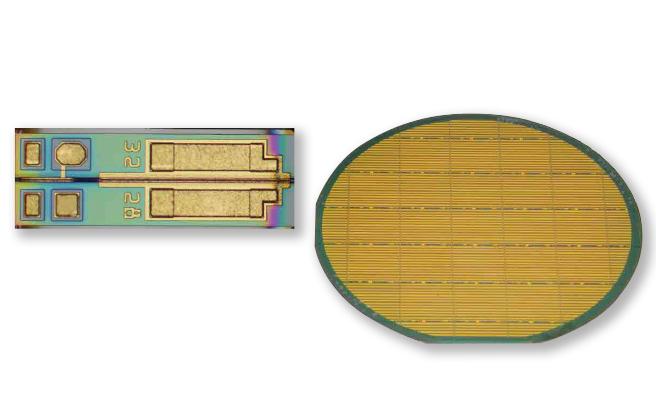
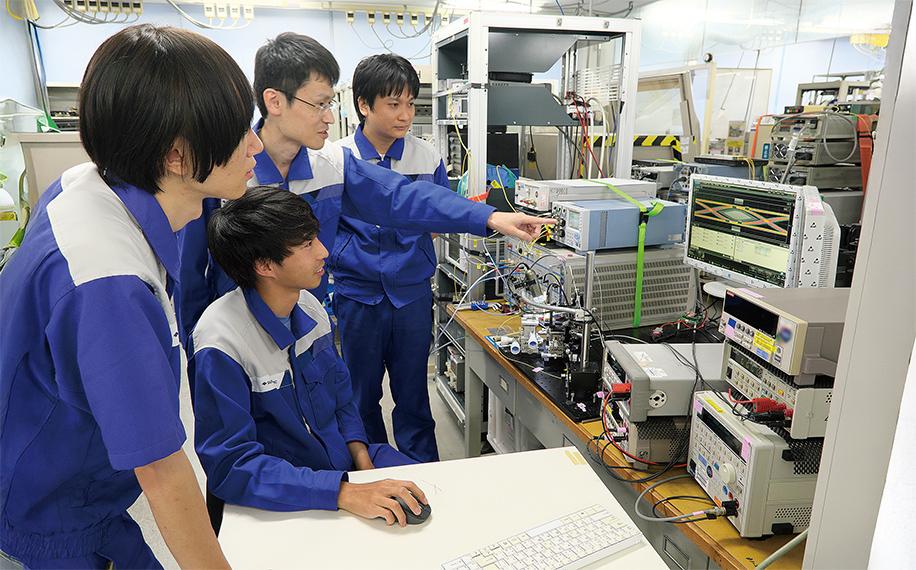
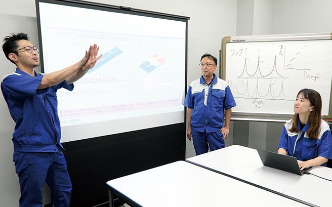
The EML, one of SEDI's main products, is an integration of a semiconductor laser that can stably emit light of a single wavelength (color) and an EA modulator. The conventional method of directly modulating the current flowing through a semiconductor laser to switch it on and off at high speed had a problem with signal degradation. The EA modulator was developed to solve this problem. This device prevents signal degradation by quickly switching between transmitting and blocking laser light. The EML has always been required to be faster and consume less power. Kyohei Maekawa of the Photonic Devices Design Department is in charge of design in the Lightwave Device Division.
"To achieve higher speeds, it is essential to reduce the electrostatic capacitance of the modulator. For that purpose, shortening the modulator length is effective, but this creates a trade-off. Doing so results in a weaker signal, which leads to communication errors. Our goal is to achieve both speed and signal integrity by devising the internal structure of the EA modulator. Semiconductor lasers emit light using extremely small electron wells, called 'quantum wells'. By stacking them together to create multi-quantum wells and optimizing their structure, it becomes possible to emit light faster and more efficiently, so we are also working on developing this." (Maekawa)
Differential Drive — A New EML Driving Method
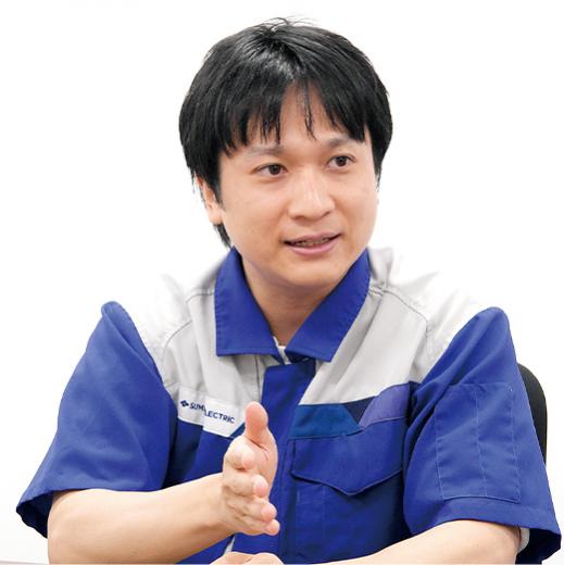
Masahiro Honda of the Product Development Department is in charge of project management, listening to customer needs and incorporating them into products. He is currently focusing on the development of a new method called "differential drive EML." Driving refers to supplying electrical signals from outside to make the optical device operate correctly.
"Conventionally, EA modulators were driven by a single electrical signal. The differential drive EML is an improvement that allows it to be driven by two electrical signals. The background to this development was customer requests for higher speeds and lower power consumption. Using two electrical signals makes it possible to suppress the effects of external noise, which become more noticeable as speeds increase. Furthermore, the amplitude of the electrical signal can be reduced, which implies the possibility of reducing power consumption." (Honda)
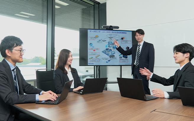
The differential drive EML is important in fields such as data centers that require high speed and energy efficiency. The device will continue to be improved as it incorporates feedback from customers, with the goal of achieving mass production.
CW-LD Aiming for High Output and Low Power Consumption
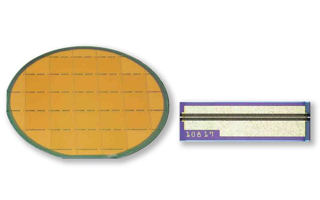
One of SEDI’s other main products, the CW-LD, which is becoming a major player in the data center market, is designed by Konosuke Aoyama of the Photonic Devices Design Department. The CW-LD is a semiconductor laser that constantly emits a certain light. Without having an internal modulator, the device performs the conversion to an optical signal using an external modulator. Aoyama is working on how to achieve even greater output more efficiently.
"Current leakage is always an issue when increasing power output. It causes a significant decrease in power conversion efficiency. To reduce current leakage, we precisely controlled the temperature and gas ratio during crystal growth on the substrate and repeatedly studied the types and amounts of impurities required. In addition, we increased the width of the active layer that emits light so as to obtain light more efficiently, and in parallel with this, by isolating areas with different electrical functions, power distribution has been optimized. As a result, high optical output and power conversion efficiency have been achieved. We are already in the phase of preparing for mass production." (Aoyama)
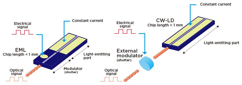
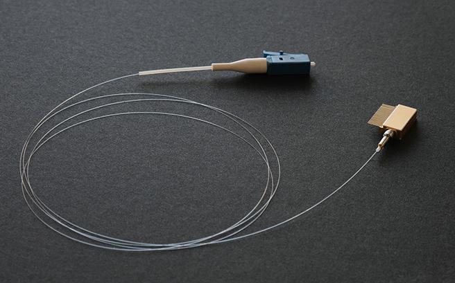
A laser chip is a semiconductor chip that converts electricity into light. There are two types: the EML, which has an internal modulator (shutter) that can switch the light on and off and can independently convert electrical signals into optical signals. By contrast, the CW-LD has no internal modulator; it emits a continuous light and uses an external modulator to convert the light into optical signals.
Compound Semiconductor Substrates (Wafers): A Challenge for High Quality and Precision
— Sumiden Semiconductor Materials Co., Ltd.
The quality of semiconductor lasers used in optical communications depends heavily on the quality of the wafer. The wafers are produced by thinly slicing an ingot, a column of grown indium phosphide crystals. The company responsible for the manufacturing and development of these compound semiconductor substrates is Sumiden Semiconductor Materials Co., Ltd. Yuichi Oeki of the Itami Crystal Production Engineering Group is in charge of the crystal growth process in wafer manufacturing.
"The materials are indium and phosphorus. They are subjected to a thermal reaction, melted at high temperatures to create a liquid, and then cooled to form single-crystal indium phosphide. My mission is to optimally control and manage high temperatures of over 1,000°C inside the crystal growth furnace to produce high-quality single-crystal indium phosphide. I continue to improve that process every day." (Oeki)
The ingot produced in this way is then sliced. The role of Tomoki Kimura of the Processing and Production Engineering Group is responsible for slicing the ingot.
"The ingot is brittle and easily chipped. Slicing at a scale of 0.5 mm to 0.8 mm, along with the subsequent chamfering process, requires meticulous attention. At the same time, maintaining the orientation of the crystal lattice, which indicates the crystal orientation of the wafer, is crucial during the manufacturing process. As it serves as a reference for processing, I am always striving to achieve high precision." (Kimura)
For Ryo Takasaki of the Facilities Group, the most important task at present is the installation of crystal growth furnaces.
"We have a number of crystal growth furnaces, but as demand for optical devices is growing rapidly, we are considering the introduction of additional furnaces. Crystal growth furnaces, which are used under high temperatures and pressures, require comprehensive safety measures, and there is also a requirement for technology to measure the temperature inside the furnace more accurately during crystal growth." (Takasaki)
Sumiden Semiconductor Materials Co., Ltd. continues to take on the challenge of upgrading its capabilities with more advanced facilities and pursuing the production of even higher-quality wafers.
NEXT
Process Development for Mass Production of Optical Devices
- Developing Process Technologies for New Products -

Registration of public notification
If you register your e-mail address, we will notify you when the latest issue is published. If you wish, please register from the registration form.
To delete your registration, please visit here.