
Process Development for Mass Production of Optical Devices
Developing Process Technologies for New Products
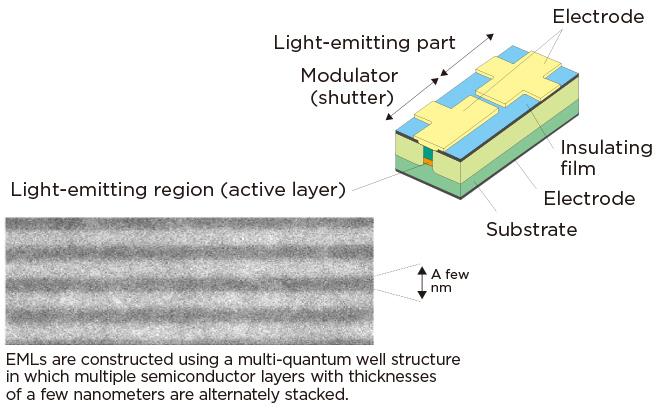
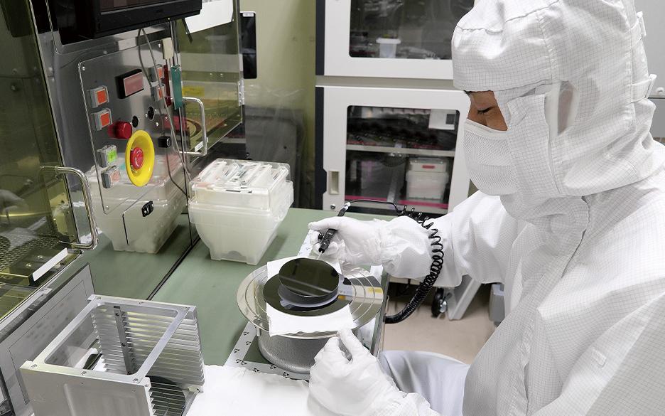
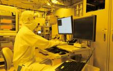
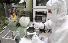
Epitaxial Growth and Dry Etching
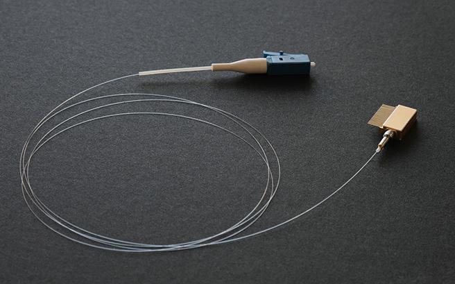
Product specifications presented during the design stage are translated into a concrete form through process development, which is the source of SEDI's strength. One aspect of process development is the epitaxial growth of compound semiconductors. This technology involves forming and layering new thin crystal layers on top of a crystal substrate (wafer) in a way that precisely traces the crystalline structure of the substrate. This technology enables the creation of high-quality semiconductor layers with specific functions. The process is to form nanometer-scale thin films by transporting an organometallic raw material in conjunction with a gas that moves the raw material to a crystal growth furnace, where the material is thermally decomposed on a crystal substrate heated to approximately 600°C. Consequently, temperature and pressure control and appropriate gas selection have a significant impact on the crystal quality. SEDI has developed epitaxial growth technology over many years, enabling the formation of high-quality thin films with high precision and uniformity.
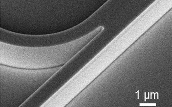
Dry etching proceeds in tandem with this process. Developed specifically for miniaturizing laser chips, this technique uses gas and plasma to etch the substrate, achieving high-precision fabrication of intricate circuit patterns according to the design. SEDI possesses unique technologies that utilize dry etching to create smooth fine optical paths and precisely process distinctive structures, making them core technologies of SEDI alongside epitaxial growth technology.
Achieving Improved Characteristics with Novel Compound Semiconductors
Tohma Watanabe of the Device Process Engineering Department has been in charge of epitaxial growth since joining the company. He has worked continuously on epitaxial growth technology since his student days.
"The manufacturing process for optical devices consists of repeated cycles of epitaxial growth and etching, known collectively as the growing and engraving process. I have been working on improving the characteristics of EML. Making the light flash faster and sending clearer signals leads to faster optical communication. The key is how much light the modulator can absorb.Finding the optimal compound for the modulator's multi-quantum well structure was very difficult, but I persevered in process development and was able to proceed to mass production." (Watanabe)
Having achieved the optimization of the multi-quantum well structure, Watanabe aims to become a semiconductor manufacturing professional by mastering the process of epitaxial growth.
Transition from 2-Inch Wafers to 4-Inch Wafers
Takumi Endo, who belongs to the same Device Process Engineering Department as Watanabe, is also involved in process development. A turning point for him as an engineer working with optical devices was the expansion of wafers to 4-inch ones used in the manufacturing of laser chips.
"If the diameter is larger, many chips can be cut from one wafer. This allows us to achieve lower costs. However, changing the diameter necessitated a review of the equipment and manufacturing conditions, and I continued to optimize the process by tackling each challenge. Currently, 4-inch wafers are already in mass production and are one of the key sources of our competitiveness." (Endo)
Endo is also in charge of launching 4-inch wafers for the mass production of high-light output CW-LDs. The challenge for him is laser chip miniaturization. By achieving this, he aims to contribute to cost reduction.
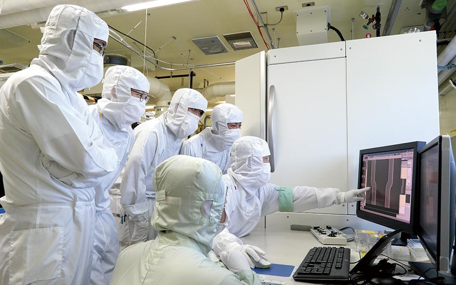
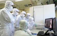
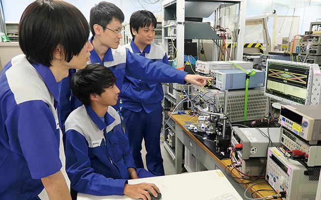
Aiming to Optimize and Stabilize Production Facilities
Takuma Sekiguchi, who belongs to the Manufacturing Engineering Department, is in charge of preshipping inspection of mass-produced optical devices. His tasks go beyond merely judging products as pass or fail.
"Due to the surge in demand, our existing facilities cannot keep up, so we are implementing a plan to increase production. It takes about six months, including trial runs, for the equipment to be installed and operate stably. Another significant challenge is how to minimize the defect rate and reduce waste. Through various explorations, we hope to achieve optimization and stabilization not just in inspection, but also in production equipment, as well as cost reduction." (Sekiguchi)
The team members continue to work hard amid the dramatic changes in the environment surrounding optical devices, including the need to respond quickly to the surge in demand and swift process development to meet the demands for new product development.


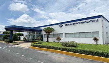
Overseas Manufacturing Sites Efforts in Vietnam
—Sumiden Device Innovations Vietnam Co., Ltd.
SEDI's manufacturing sites are located in Yokohama and Yamanashi, along with an overseas site near Ho Chi Minh City, Vietnam. Sumiden Device Innovations Vietnam Co., Ltd. (SEDV) is responsible for the production of optical modules that incorporate laser chips made by SEDI. SEDV's main products are characterized by their small size, high optical output, and low power consumption. For example, a package about the size of a smartphone's nanoSIM card (the smallest SIM card) is assembled with approximately 20 components with extremely fine precision utilizing various joining technologies. At SEDI, the development and manufacturing staff work together, focused on ensuring stable mass production; SEDV has taken further steps to thoroughly enhance its assembly and inspection methods, thus achieving shorter times and increased production. The individual overseeing all of this is General Director Motoki Saji.
"Looking ahead, I believe it is important to consider about how to manufacture products efficiently. While solidifying our foundation and actively incorporating innovative ideas and technologies that look forward the future, we aspire to make a significant contribution as a key manufacturing hub for high-performance optical modules." (Saji)
SEDV strongly supports SEDI by promoting efficient production and by ensuring the stability and improvement of both mass production and production ramp-up framework.
NEXT
Forefront of Optical Device Research
- Heterogeneous Integration Technology and Photonic Crystal Surface-Emitting Laser -

Registration of public notification
If you register your e-mail address, we will notify you when the latest issue is published. If you wish, please register from the registration form.
To delete your registration, please visit here.