
The Evolution of Optical Devices Essential for Optical Communications
Responding to the New Demands of Data Centers
Semiconductor Lasers for Transmission: Essential Devices for High-Speed, High-Capacity Communications
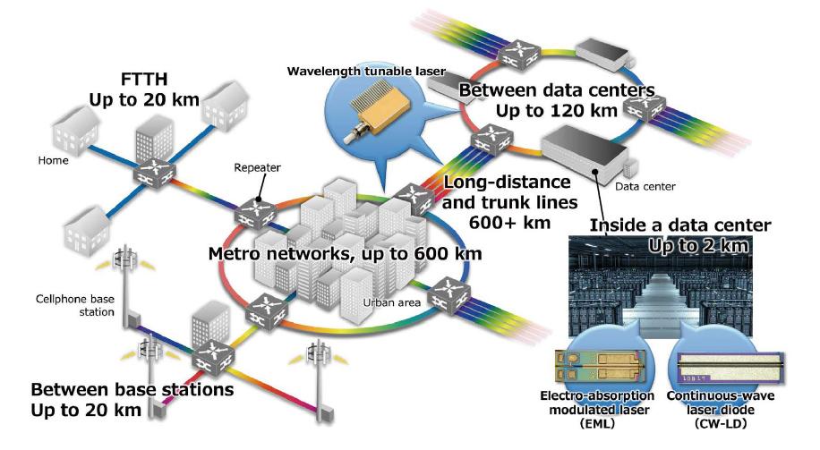
Optical communication has now become an important component of social infrastructure, benefiting many people. To handle growing data traffic, a shift from metal cables to optical fiber cables has occurred because the latter allows for the stable transmission of large volumes of data at high speeds over long distances. In optical communications, signals are converted from electrical to optical at the transmitting end, transmitted over optical fibers, and then converted back to electrical signals by a photodetector at the receiving end.
The critical factor is the light source. Currently, the light source used in optical communications is the semiconductor laser, which is a light-emitting element. The light source, emitting light with the same wavelength and phase, enables stable data transfer over long distances at high speeds. This is the optical device that the Sumitomo Electric Group has been developing and manufacturing for many years.
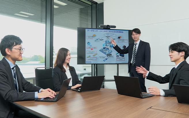
As communication traffic increases at data centers, there is a demand for the data center to handle faster, higher-capacity communication while reducing its power consumption.
AI Solutions Created by Extraordinary Processing Power
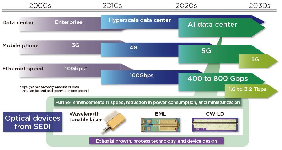
With the advent of generative AI, data centers are shifting to become AI data centers. The biggest difference compared to conventional data centers is the high processing power needed for AI computations. AI data centers are equipped with hardware specifically designed for AI, such as graphics processing units (GPUs), that enable rapid learning and analysis of large amounts of data. The volume of data and computations that companies and research institutions need to process is increasing exponentially; optical devices are essential components for transmitting this massive volume of data quickly and reliably.
Three Key Products Supporting Data Centers
Sumitomo Electric Device Innovations, Inc. (SEDI) is responsible for the optical device business of the Sumitomo Electric Group. SEDI has two domestic business sites in Yokohama and Yamanashi. In addition, it has a manufacturing site in Vietnam and development support divisions in Europe, the United States, and China, where the company designs, develops, and manufactures optical and wireless communication devices. The source of its strength is its ability to provide both optical and wireless communication solutions from a single company, from raw material development to final products. The person who leads SEDI is President & CEO Hirotake Iwadate. He has worked on optical devices since joining the company and assumed his current position in June 2025.
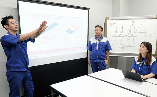
"The explosive increase in data traffic requires optical devices that enable high-speed, high-capacity data transmission. We have responded quickly and effectively. We specialize in optical communication devices that connect devices within data centers and among data centers. Electroabsorption modulated lasers (EML) and continuous-wave laser diodes (CW-LD) (details below) are used within the data centers. In addition, we supply tunable lasers that can simultaneously send multiple wavelengths of light over optical fibers between data centers. The EML is a product with a history of approximately 40 years, and we are among the leaders in the global EML market. The CW-LD has achieved high levels of efficiency, high output, and small chip size and has come to dominate the global market." (Iwadate)
High Technological Expertise Developed by Compound Semiconductors

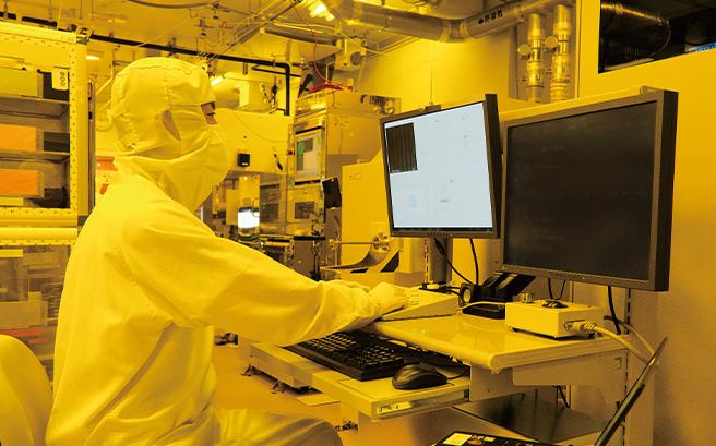
SEDI's strength, which has allowed it to maintain its competitive edge in the global market, lies in its materials. While silicon is a well-known semiconductor material, the materials used in optical devices include compound semiconductors composed of multiple elements, such as indium phosphide and gallium arsenide. Compound semiconductors enable the creation of light-emitting devices and high-performance electronic devices that cannot be achieved with silicon, which is a single-element semiconductor. The process used for the crystal growth of these compound semiconductors is known as epitaxial growth (details below). SEDI has been refining this technology for about half a century.
"Compound semiconductor optical devices are continually required to achieve higher speeds, capacities, and lower power consumption, and this demand continues to this day. Data communication speeds, which used to be around 10 Gbps, have now increased to 800 Gbps, with 1.6 Tbps on the horizon in the near future. To achieve even higher performance, there is a multitude of technical challenges that must be addressed. We want to bring about innovation while approaching the market and our customers with sincerity." (Iwadate)
Iwadate continues to explain SEDI’s vision.
"The optical communications market is characterized by repeated cycles of growth and stagnation. Nonetheless, we take pride in having continued to invest and hone our technology development and manufacturing capabilities even through these cycles. We will continue to maximize the advantages of compound semiconductors and to supply high-value-added products." (Iwadate)
NEXT
Effectively Responding to Market Demands with New Devices
- Trends in EML and CW-LD Development -

Registration of public notification
If you register your e-mail address, we will notify you when the latest issue is published. If you wish, please register from the registration form.
To delete your registration, please visit here.