

From a Local Electronics Shop to a Workplace Where Uncompromising Quality Matters for Lives
My roots lie in a neighborhood electronics store run by my family. Since childhood, I helped with air conditioner installation and electrical work. Perhaps because I grew up in that environment, although I attended a regular high school, when it came time to consider employment, I joined Sumitomo Electric because I was familiar with a company that handles electrical wires.
When I joined the company, I thought the main focus was on electric wires and automotive-related fields. However, during a recruitment briefing session, I learned that the company also had a medical business, which piqued my interest and led me to apply. That was the Medical Electronics (ME) Group at the System Equipment Plant. My responsibilities included the manufacturing and development of artificial blood vessels and sensors that measure carbon dioxide and oxygen levels inside blood vessels. Medical devices, particularly artificial blood vessels, are products that directly impact patients’ lives. Even the slightest foreign matter contamination is unacceptable. Although this development department no longer exists, the commitment to absolute quality that I learned there formed the initial foundation of my career as an engineer.
After that, I was transferred to the research and development department and entered the world of surface treatment (plating), where I experienced a major culture shock. At the manufacturing site, the priority was to produce zero defects, but in research and development, deliberately failing was part of the job in order to find a solution. I learned the importance of trying countless conditions and finding the path to the solution from failure data.
I believe that experiencing two completely different approaches—the rigor of the manufacturing floor and the inquisitiveness of research and development—has become the foundation of who I am today as an engineer.
Visualizing the Invisible World
In particular, the development of flexible printed circuits (FPC) was a major turning point for me. These circuits, which bend intricately inside smartphones and PCs, require advanced plating technology. Initially, there were many defects, and it was difficult for the product to take shape as a tangible item. Slight differences in pretreatment, plating thickness, and shape all interacted in complex ways. Therefore, we established a pilot plant, which precedes mass production, to thoroughly examine all conditions.
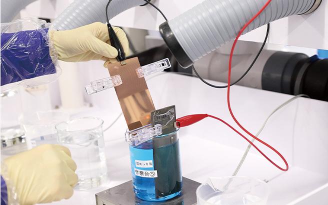
Plating is a technology that creates a metal film on the surface of metal products to enhance their performance, durability, and safety. By immersing the product in a solution containing metal ions of the plating metal and applying an electric current, tiny metal particles adhere to the surface, forming a film at micron scale. This process is a battle fought within an “invisible world.”
The temperature, concentration of the solution, along with pretreatment interact in complex ways. Even when the calculated conditions are the same, it is commonplace for the actual results on site to be completely different. Even when research staff say “theoretically, it should be like this,” when we actually try it, the way bubbles form is different or the voltage becomes unstable.
In such instances, I would never simply say, “I couldn’t do it.” Instead, I always report any unusual observations from the site, such as “this is the reaction we’re seeing here” or “the bubbles are coming out differently than usual.”
Sometimes we close the gap between theory and reality through discussion. After all the trial and error, when a mass production plant is finally completed and the product is released to the market, I feel a deep sense of pride as an engineer.
If I had to describe my job in one sentence, I would say it’s about making the invisible plating process visible. Experiments that succeed at the lab level in a beaker are pointless if they can’t be scaled up to mass production. In mass production environments, a system is needed that allows for the consistent production of high-quality goods, even if workers aren’t highly skilled. Therefore, rather than relying on experience alone, we clearly define numerical targets like “temperature at X degrees and process time of Y seconds.” In short, it is important to establish standards for mass production. My role is to act as a bridge between researchers, who create the initial prototype, and mass production plants, which scale it up reliably; that is, to ensure that the first crucial step is solid.
Staying True to the Basics and Listening to the Voice of the Object
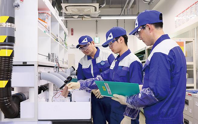
In 2023, I was certified as an Expert recognized on a company-wide basis. Currently, in addition to honing my own technical skills, I am also focusing on mentoring young engineers as an instructor at SEI University.*1
In my lectures, I teach the fundamentals of plating through practical exercises such as the Hull cell test.*2 Two things I always tell young people are to “stay true to the basics” and to “observe the object carefully.”
If you try to jump straight into applying concepts or taking shortcuts, you’ll inevitably get lost. First, faithfully adhere to the basic conditions exactly as you were taught. Then, carefully observe the reactions taking place in the solution—the size of the bubbles, changes in color, and sounds. I believe that true adaptability, the ability to handle irregular situations, is only acquired when you can perceive the messages from materials that don’t show up in data.
Going forward, I want to not only focus on plating itself but also deepen my skills in areas such as evaluating the quality of plating—for example, crosssectional observation and polishing. Furthermore, even when I receive requests for work in areas I haven’t yet experienced, such as automotive parts and wiring harnesses, I want to continue to be a versatile engineer who people can rely on: “If we leave it to Ueda, he’ll figure something out.”
I continue to take steps toward establishing standards by making the invisible microscopic world visible. This is the challenge.
*1: SEI University is the collective name for the education and training programs of the Sumitomo Electric Group.
*2: The Hull cell test is an electrodeposition plating test that uses a small trapezoidal test bath (Hull cell). This test quickly visualizes the plating bath condition using a small volume of plating solution.
PROFILE
Takeshi Ueda
1992
Joined Sumitomo Electric Industries, Ltd.
1993
Medical Electronics Group, System Equipment Plant (CO2 sensors, artificial blood vessel manufacturing, inspection, and sterilization)
1994
Biomaterials Group, Section 3, Osaka Administrative Section (Artificial blood vessel manufacturing and development)
2003
Electrochemistry Group, Section 2, Osaka Support Group, Research Planning Department (Development of aluminum Celmet products, defect mitigation measures for Ni Celmet)
2011
Instructor for the practical technology training for stabilizing plating quality at Itami TTC
2022
Electrochemistry Group, Section 2, Osaka Support Group, Development Operation Department, R&D Planning & Administration Division (Development of and defect mitigation measures for FPC board products)
2023
Company-wide Expert* certification
* Expert: Sumitomo Electric focuses on the skills that underpin the core of its manufacturing process. To maintain, improve, and ensure the succession of these skills, it certifies employees with essential skills as Experts.


